Close Menu
  • Analog Design
    • Latest Analog Layout Interview Questions (2025)
  • Digital Design
    • Digital Electronics Interview Question(2025)
    • Top VLSI Interview Questions
  • Physical Design
    • Physical Design Interview Questions for VLSI Engineers
  • Verilog
    • Verilog Interview Questions(2024)
  • Forum
Facebook Instagram YouTube LinkedIn WhatsApp
SiliconvlsiSiliconvlsi
Forum Questions Register in Forum Login in Forum
Facebook Instagram YouTube LinkedIn WhatsApp
  • Analog Design
    • Latest Analog Layout Interview Questions (2025)
  • Digital Design
    • Digital Electronics Interview Question(2025)
    • Top VLSI Interview Questions
  • Physical Design
    • Physical Design Interview Questions for VLSI Engineers
  • Verilog
    • Verilog Interview Questions(2024)
  • Forum
SiliconvlsiSiliconvlsi
Home»Analog Design»Analog Layout Design-Improve Parasitic Capacitance in IC layouts
Analog Design

Analog Layout Design-Improve Parasitic Capacitance in IC layouts

siliconvlsiBy siliconvlsiMarch 14, 2022Updated:May 12, 2024No Comments2 Mins Read
Facebook Pinterest LinkedIn Email WhatsApp
Share
Facebook Twitter LinkedIn Pinterest Email

Parasitic Capacitance in IC Layouts

Parasitics can be of resistance or capacitance types, or both. As the semiconductor industry is growing so does the density of devices on-chip. The parasitic capacitance arises from an electrical coupling between one signal line and another signal line or a signal line and the substrate. With the increasing density and decreasing spacing rules, the most significant effect that comes into the picture is parasitic capacitance. At low frequencies, parasitic capacitance can usually be ignored, but in high-frequency circuits, it can be a major problem.

Parasitic Capacitance in IC layouts

Origin of parasitic capacitance

  • Diffusion to substrate
    • Side-wall capacitance-capacitance from the periphery
    • bottom-wall capacitance-capacitance to the substrate
  • Metal to substrate
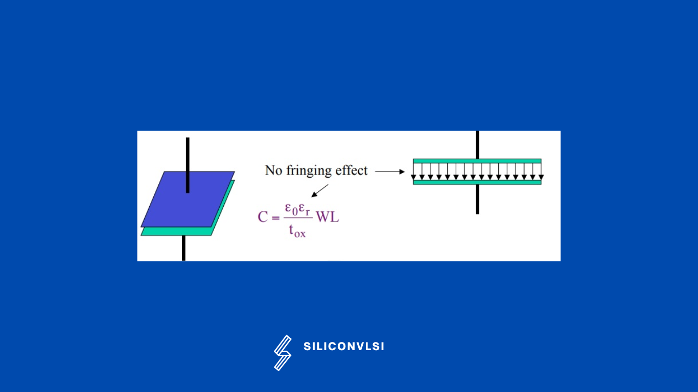
    • Parallel plate capacitance is dominant
    • Need to account for fringing, too
  • Poly to substrate
    • Parallel plate plus fringing, like metal
    • don’t confuse poly over a substrate with the gate capacitance
  • Capacitance between conductors
    • Metal 1 &  Metal2
    • Metal2 & Metal3

The best method for decreasing parasitic capacitance

  • Avoid too much parallel routing of metals.
  • Increasing the spacing of all the nets from the net is critical
  • Use higher metals for the net in which parasitic capacitance is important.
  • Put some other reference signal or dummy signal in between the nets for which lower parasitic capacitance is required. This is also called shielding.

How can parasitic capacitance be prevented?

Careful separation of components and wires, including the use of guard rings, power planes, ground planes, and shielding between output and input, along with proper termination of transmission lines, is essential to minimize unwanted parasitic capacitance.

Share. Facebook Twitter Pinterest LinkedIn Tumblr Email

Related Posts

BJTs vs. MOSFETs: Key Differences Every Analog Designer Should Know

April 3, 2025

Understanding the 2.5D Approach in Packaging Technology

December 1, 2024

Essential Analog Layout Interview Questions: Unveiling Key Insights

August 3, 2024
Leave A Reply Cancel Reply

Facebook X (Twitter) Instagram Pinterest Vimeo YouTube
  • About Us
  • Contact Us
  • Privacy Policy
© 2025 Siliconvlsi.

Type above and press Enter to search. Press Esc to cancel.