
Logical Left Shift Barrel Shifter
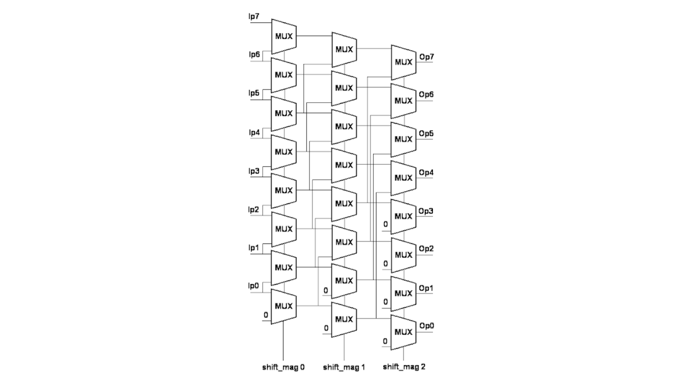
A logical left-shift barrel shifter is a digital circuit that can shift an 8-bit data word to the left by a specified number of bits in one clock cycle. The block diagram of the logical left-shift barrel shifter is shown in Figure 1.
Verilog Module: Logical Left Shift Barrel Shifter
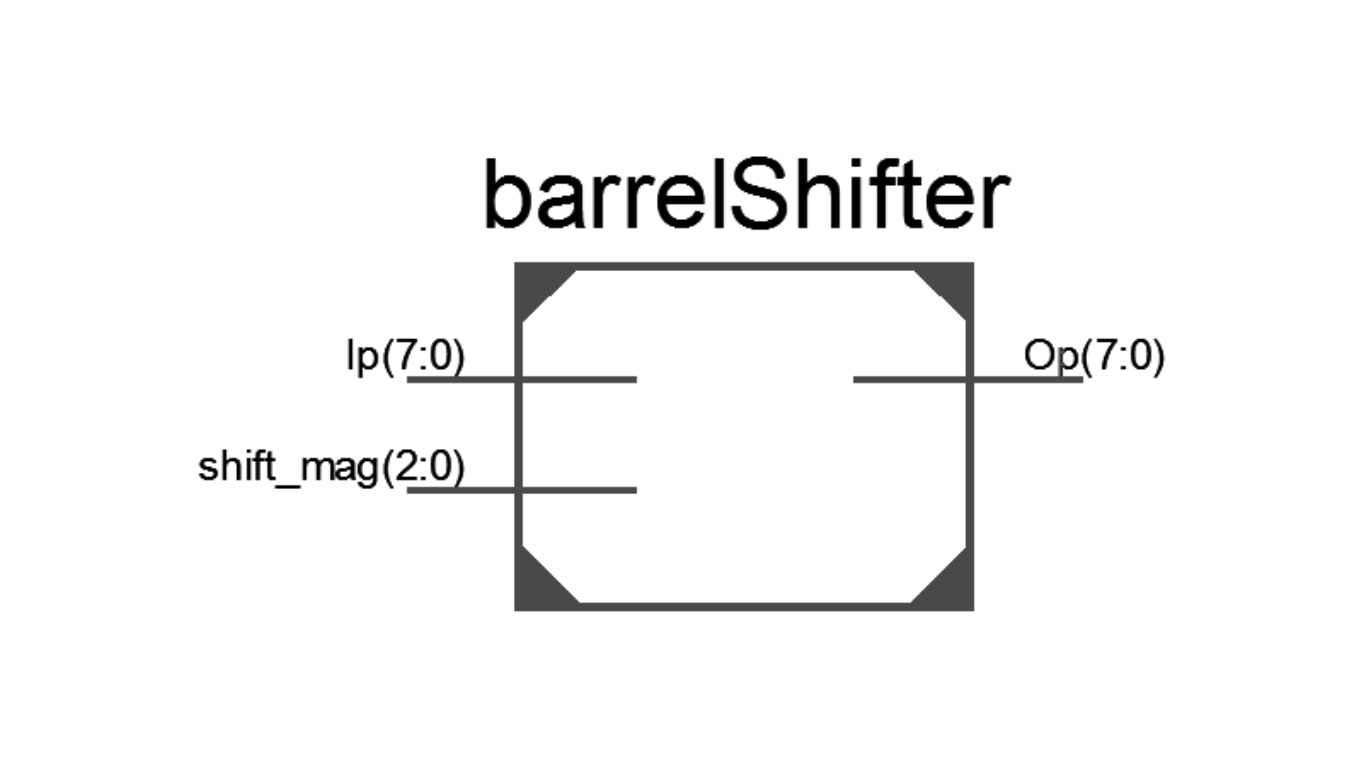
The Verilog module of the logical left-shift barrel shifter is shown in Figure 2. It has one 8-bit input port, Ip, and a 3-bit port shift_mag for the left shift magnitude. The module presents the 8-bit shifted value from the output port Op
Verilog Code for the 8-bit Logical Left Shift Barrel Shifter
module barrelShifter(
input [7:0] Ip, // The 8-bit Input line
output [7:0] Op, // The 8-bit Output line
input [2:0] shift_mag // The 3-bit shift magnitude selection Input
);
wire [7:0] ST1, ST2; // Two 8-bit intermediate lines.
// The barrel shifter implemented as an array of MUXes
mux_2to1 m0 (1’b0, Ip[0], ST1[0], shift_mag[0]);
mux_2to1 m1 (Ip[0], Ip[1], ST1[1], shift_mag[0]);
mux_2to1 m2 (Ip[1], Ip[2], ST1[2], shift_mag[0]);
mux_2to1 m3 (Ip[2], Ip[3], ST1[3], shift_mag[0]);
mux_2to1 m4 (Ip[3], Ip[4], ST1[4], shift_mag[0]);
mux_2to1 m5 (Ip[4], Ip[5], ST1[5], shift_mag[0]);
mux_2to1 m6 (Ip[5], Ip[6], ST1[6], shift_mag[0]);
mux_2to1 m7 (Ip[6], Ip[7], ST1[7], shift_mag[0]);
mux_2to1 m00 (1’b0, ST1[0], ST2[0], shift_mag[1]);
mux_2to1 m11 (1’b0, ST1[1], ST2[1], shift_mag[1]);
mux_2to1 m22 (ST1[0], ST1[2], ST2[2], shift_mag[1]);
mux_2to1 m33 (ST1[1], ST1[3], ST2[3], shift_mag[1]);
mux_2to1 m44 (ST1[2], ST1[4], ST2[4], shift_mag[1]);
mux_2to1 m55 (ST1[3], ST1[5], ST2[5], shift_mag[1]);
mux_2to1 m66 (ST1[4], ST1[6], ST2[6], shift_mag[1]);
mux_2to1 m77 (ST1[5], ST1[7], ST2[7], shift_mag[1]);
mux_2to1 m000 (1’b0, ST2[0], Op[0], shift_mag[2]);
mux_2to1 m111 (1’b0, ST2[1], Op[1], shift_mag[2]);
mux_2to1 m222 (1’b0, ST2[2], Op[2], shift_mag[2]);
mux_2to1 m333 (1’b0, ST2[3], Op[3], shift_mag[2]);
mux_2to1 m444 (ST2[0], ST2[4], Op[4], shift_mag[2]);
mux_2to1 m555 (ST2[1], ST2[5], Op[5], shift_mag[2]);
mux_2to1 m666 (ST2[2], ST2[6], Op[6], shift_mag[2]);
mux_2to1 m777 (ST2[3], ST2[7], Op[7], shift_mag[2]);
endmodule
Verilog Code of the Test Bench for Logical Left Shift Barrel Shifter
The Verilog test bench for the logical left-shift barrel shifter is shown in Figure 4. It tests the functionality of the barrel shifter by providing stimulus to the input ports (Ip and shift_mag) and observing the output port Op.
module barrelShifter_tb;
// Inputs
reg [7:0] Ip;
reg [2:0] shift_mag;
// Outputs
wire [7:0] Op;
// Instantiate the Unit Under Test (UUT)
barrelShifter uut (
.Ip(Ip),
.Op(Op),
.shift_mag(shift_mag)
);
initial begin
// Initialize Inputs
Ip = 8’d0;
shift_mag = 3’d0;
// Wait 100 ns for global reset to finish
#100;
// Add stimulus here
Ip = 8’d16;
shift_mag = 3’d2;
#20;
Ip = 8’d4;
shift_mag = 3’d2;
end
endmodule
Timing Diagram for Logical Left Shift Barrel Shifter
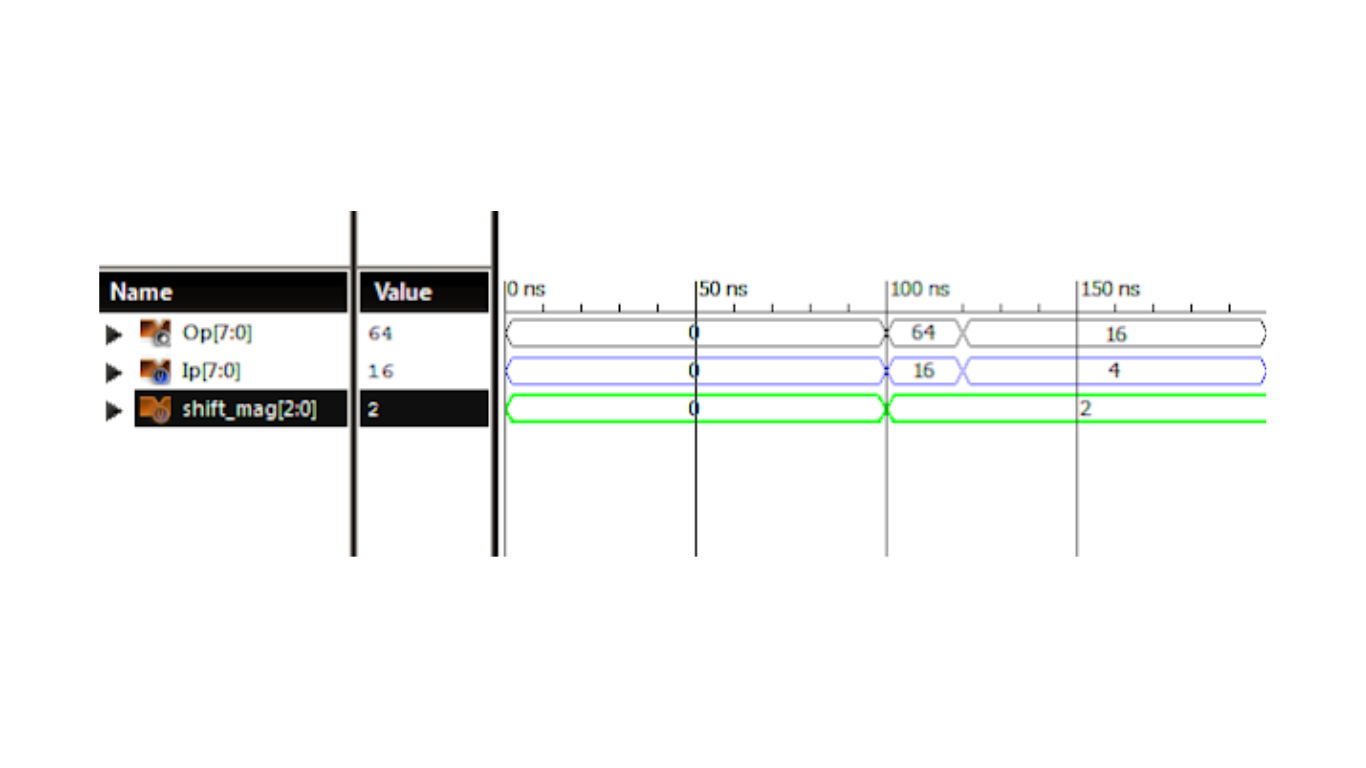
Figure 5 presents the timing diagram of the logical left shift barrel shifter, illustrating the waveforms of the output Op as the input data is shifted to the left based on the shift_mag input. The barrel shifter efficiently performs the left shift operation in a single clock cycle.
The provided Verilog module and test bench ensure the correct functionality of the logical left-shift barrel shifter for different shift magnitudes.