
MOSFET
The MOSFET, a four-terminal semiconductor device, serves as an essential component in modern electronics. Its behavior can be understood at a basic level as a switch controlled by the voltage applied to its gate terminal. Here are key characteristics and distinctions:
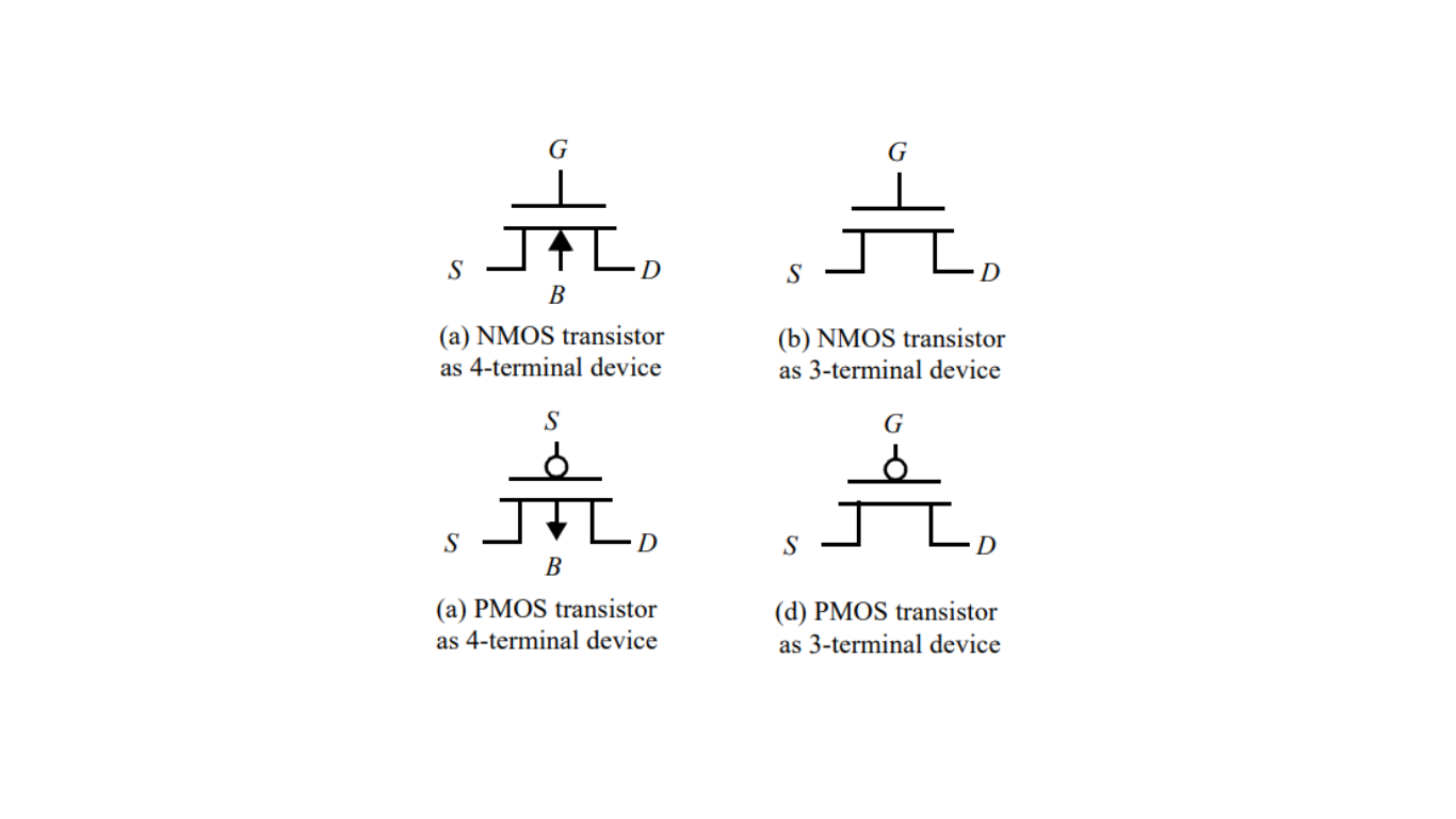
Four-Terminal Device: The MOSFET comprises four terminals – gate, source, drain, and body. The gate voltage regulates the flow of current between the source and drain terminals, with the body terminal playing a secondary role in modulating device parameters.
Switch-Like Operation: At its simplest, a MOSFET acts as a switch. When the gate voltage surpasses a specific threshold voltage (VT), it creates a conductive channel between the source and drain. With a voltage difference between the source and drain, current flows through this channel. Higher gate-source voltage increases channel conductivity, resulting in greater current. Conversely, when the gate voltage is below VT, no channel exists, and the MOSFET behaves as an open switch.
Two Types: MOSFETs come in two primary types – NMOS and PMOS. In NMOS, the source and drain regions are n+ doped, situated within a p-type substrate. Electrons carry the current through an n-type channel. In contrast, PMOS employs p+ doped source and drain regions in an n-type substrate, with current conveyed by holes through a p-type channel. Complementary MOS technology (CMOS) combines both NMOS and PMOS devices for diverse applications.
Circuit Symbols: Circuit symbols depict MOSFETs as four-port devices, representing the gate, source, drain, and body terminals. Often, the body terminal connection is implied since it typically connects to a common supply (e.g., GND for NMOS, Vdd for PMOS). When not explicitly shown, it’s assumed the body is appropriately connected.
In summary, MOSFETs are versatile semiconductor components serving as voltage-controlled switches. They offer advantages over diodes by allowing precise control of current flow between source and drain terminals, making them integral to modern electronics, especially in CMOS technology.
How many terminals does a MOSFET (Metal-Oxide-Semiconductor Field-Effect Transistor) have, and what is the primary function of the fourth terminal?
A MOSFET has four terminals. The fourth terminal, known as the body, primarily serves to modulate the device’s characteristics and parameters.
What determines whether a MOSFET acts as a switch and allows current to flow between the source and drain terminals?
Whether a MOSFET acts as a switch depends on the voltage applied to the gate terminal. If the gate voltage exceeds a specific value called the threshold voltage (VT), a conducting channel forms between the source and drain, allowing current flow.
How does the gate voltage affect the conductivity of the channel in a MOSFET?
The conductivity of the channel in a MOSFET is modulated by the gate voltage. A larger voltage difference between the gate and source terminals results in a smaller resistance of the conducting channel and a larger current.
What are the two main types of MOSFET devices?
The two main types of MOSFET devices are NMOS and PMOS. NMOS transistors have n+ drain and source regions and carry current through electrons in an n-type channel. PMOS transistors have p+ drain and source regions and carry current through holes in a p-type channel.
In a complementary MOS technology (CMOS), what types of MOSFET devices are used, and how are they typically represented in circuit symbols?
In CMOS technology, both NMOS and PMOS devices are used. Circuit symbols for MOS transistors typically include gate, source, and drain terminals. The body terminal is often not shown in schematics because it is connected to a common DC supply for devices of the same type.