
What is Dynamic Logic in CMOS Circuits?
Dynamic logic is a type of CMOS circuit design that relies on the dynamic storage of the output value on a capacitor to achieve high-speed operation. However, it faces a challenge due to leakage currents that can gradually degrade the stored charge and cause malfunctioning of the gate. Here’s an explanation of dynamic logic and how it addresses leakage issues:
Dynamic Logic
Operation: Dynamic logic stores the output value on a capacitor during the evaluation phase. When the pull-down network is off, the output should ideally remain precharged to VDD.
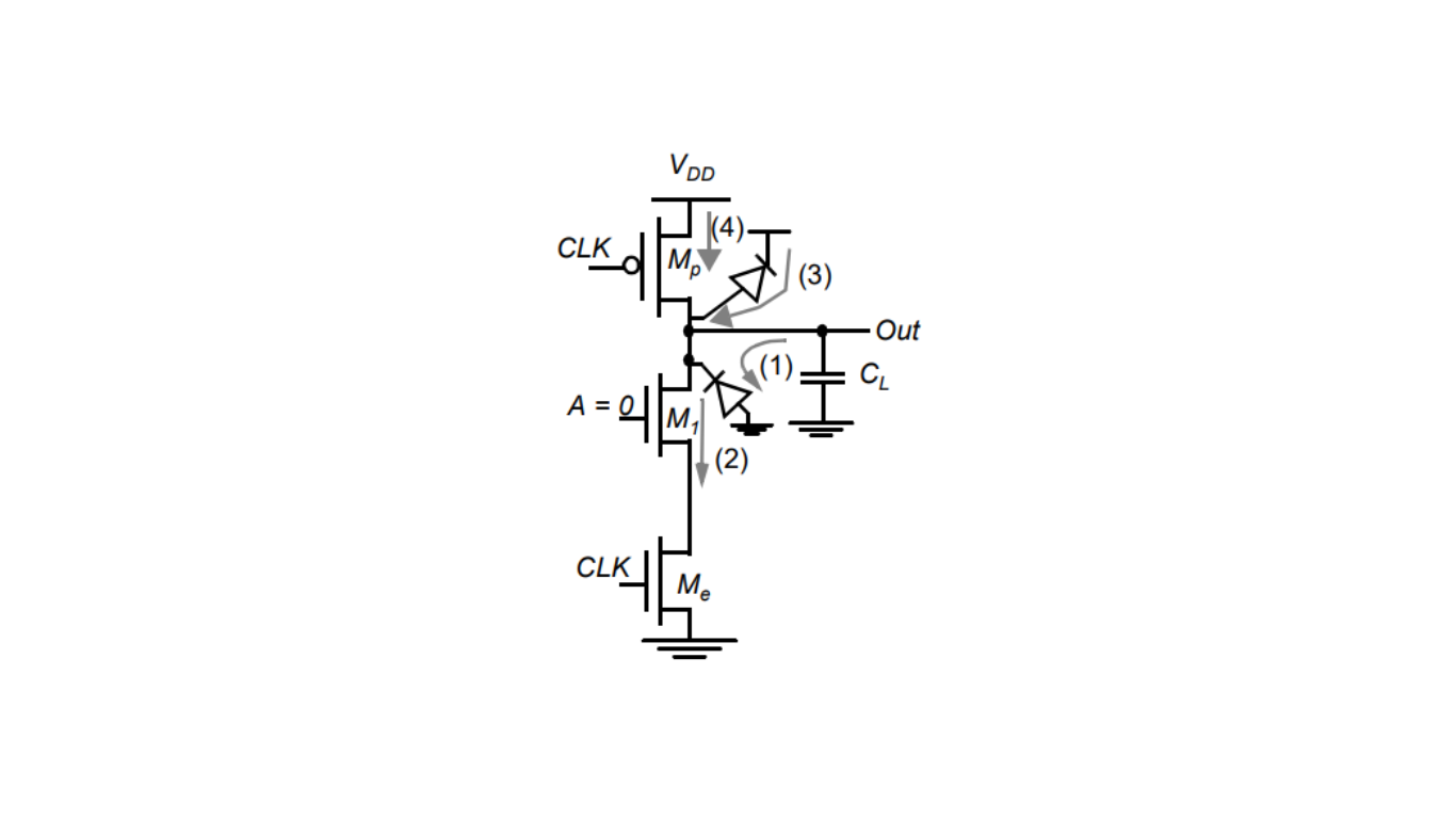
Leakage Sources: Leakage currents pose a challenge in dynamic logic circuits. There are several sources of leakage, including:
- Reverse-biased diode (Source 1)
- Sub-threshold leakage of the NMOS pull-down device (Source 2)
- Reverse bias diode and subthreshold conduction in the PMOS precharge device (Source 3 and Source 4)
Leakage Consequences: Leakage causes the charge stored on the output capacitor (CL) to gradually leak away, leading to a degradation in the high-level voltage.
Minimum Clock Rate: Dynamic circuits require a minimum clock rate (typically a few kHz) to prevent excessive leakage and maintain proper functionality.
Limitations: Due to the minimum clock rate requirement, dynamic logic is less suitable for low-performance products like watches and processors that use conditional clocks.
Bleeder Transistor
A bleeder transistor, also known as a voltage divider transistor, is a specialized type of transistor configuration used in electronic circuits, particularly in power supplies. Its primary function is to help regulate and control voltage levels in a circuit by diverting excess current away from the load or the main power transistor.
Bleeder transistors are commonly used in linear power supplies and voltage regulator circuits to improve voltage regulation. They are especially useful when dealing with varying loads and ensuring that the output voltage remains constant under different operating conditions.
Addressing Leakage with a Bleeder Transistor
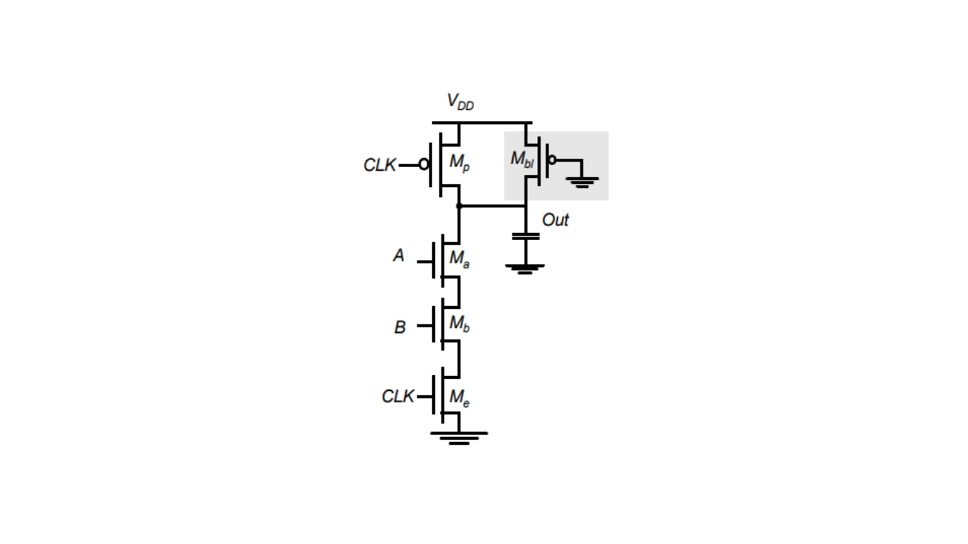
- Leakage Counteraction: To counteract leakage during evaluation, a bleeder transistor (similar to a pseudo-NMOS-like pull-up device) is often added to the dynamic logic circuit.
- Bleeder Function: The sole purpose of the bleeder transistor is to compensate for the charge lost due to pull-down leakage paths, helping to maintain the stored charge on the output capacitor.
- Reduced Output Impedance: To avoid ratio-related issues and static power consumption, the bleeder transistor is typically designed with high resistance or kept small. This allows the strong pull-down devices to lower the output voltage substantially below the switching threshold of the inverter.
- Feedback Configuration: In some cases, the bleeder is implemented in a feedback configuration to eliminate static power dissipation, further improving the energy efficiency of dynamic logic circuits.
In summary, dynamic logic achieves high-speed operation by storing the output value on a capacitor during evaluation. However, it faces leakage challenges that can degrade the stored charge. These challenges are addressed by introducing a bleeder transistor that compensates for charge loss and reduces output impedance during evaluation, ensuring the proper functioning of dynamic logic circuits.
What are the sources of charge leakage in a dynamic inverter circuit?
The sources of charge leakage in a dynamic inverter circuit include reverse-biased diodes, sub-threshold leakage in the NMOS pull-down device, and leakage in the PMOS precharge device. These leakage sources cause the charge stored on the output capacitor (CL) to gradually leak away. This leakage leads to a degradation in the high-level output.
Why do dynamic circuits require a minimal clock rate?
Dynamic circuits require a minimal clock rate because charge leakage causes a degradation in the high-level output. The typical order of magnitude for this clock rate is on the order of a few kilohertz (kHz).
How does the addition of a bleeder transistor help counteract charge leakage in dynamic circuits?
The bleeder transistor, which functions like a pseudo-NMOS-like pull-up device, compensates for the charge lost due to pull-down leakage paths during evaluation. It does so by reducing the output impedance on the output node, preventing the charge from leaking away.
What is the function of the bleeder resistance in dynamic circuits?
The bleeder resistance in dynamic circuits helps maintain the output node’s voltage during evaluation by preventing charge leakage. It is typically kept high to avoid the ratio problems associated with this circuit style and to minimize static power consumption. A high bleeder resistance allows the strong pull-down devices to lower the output node below the switching threshold of the inverter.
How is the static power dissipation associated with a bleeder transistor eliminated in dynamic circuits?
Static power dissipation associated with a bleeder transistor is eliminated by implementing the bleeder in a feedback configuration. This configuration ensures that the bleeder only operates when necessary to counteract charge leakage, reducing static power consumption when it’s not needed.