Clock Domain Crossovers
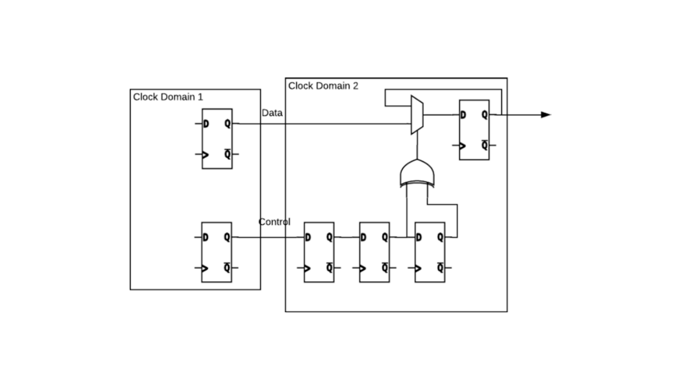
A collection of interconnected logic circuits that operate together under the control of a single clock signal is referred to as a clock domain. In modern complex System-on-Chips (SOCs), there exist numerous clock inputs that drive various segments of the logic circuitry, resulting in multiple clock domains. The primary clock is termed as such if it is produced by the clock-generating component known as the clock source. For most SOCs, the clock source is typically a Phase-Locked Loop (PLL) circuit. Conversely, a clock is considered derived if it is generated from the primary clock by internally dividing it using counters. Given the presence of multiple clock domains in a SOC, signals that undergo processing to execute specific functions traverse different clock domains. Clocks within distinct domains may possess the same frequency but different phases, or they may have different frequencies and phases. Since many logic designs rely on clock edges to drive signal changes, it is imperative to meticulously generate signals that ensure the correct data or signals are latched at the corresponding domain’s clock edge when data or signals traverse domains.

When asynchronous signals move across various clock domains, several precautions are necessary:
- Identification of Data and Control Signals: It is essential to differentiate between data and control signals. Dominant control signals must be chosen, as they dictate the behavior of the system.
- Synchronization: Asynchronous signals must be synchronized when transitioning between clock domains. The receiving clock governs this synchronization process.
- Stability and Glitch-Free Transition: Prior to the transition, the dominant control signal must be stable and free of glitches for at least one clock cycle of the receiving clock domain.
- Data Signal Stability: Data signals need to remain stable across multiple clock cycles of the receiving domain to ensure accurate processing.