
D Flip-Flop
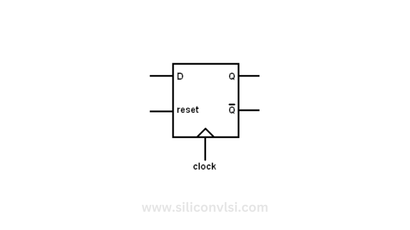
The output of a D Flip-Flop tracks the input, making transitions that match those of the input. The D in D Flip-Flop stands for Data, indicating that this Flip-Flop stores the value on the data line. It can be thought of as a fundamental memory cell. A D Flip-Flop can be created from a Set/Reset Flip-Flop by connecting the set line to the reset line through an inverter. The output of the Flip-Flop can be clocked. When the output is clocked, the D Flip-Flop becomes a synchronous D Flip-Flop. The synchronous D Flip-Flop has an output synchronized with either the rising edge or the falling edge of the input clock pulse. The block diagram of a synchronous D Flip-Flop is depicted in Figure 1.
Truth Table of a D Flip-Flop
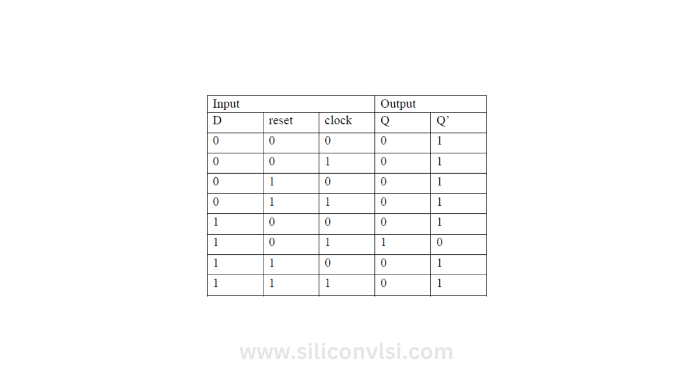
Figure 2 illustrates the truth table of a synchronous D Flip-Flop that is clocked at the rising edge of the input clock. The inputs to the D Flip-Flop are the data bit D and the control lines reset and clock. There are two outputs, Q and Q’s, which represent the complement of Q.
Verilog Module of a D Flip-Flop
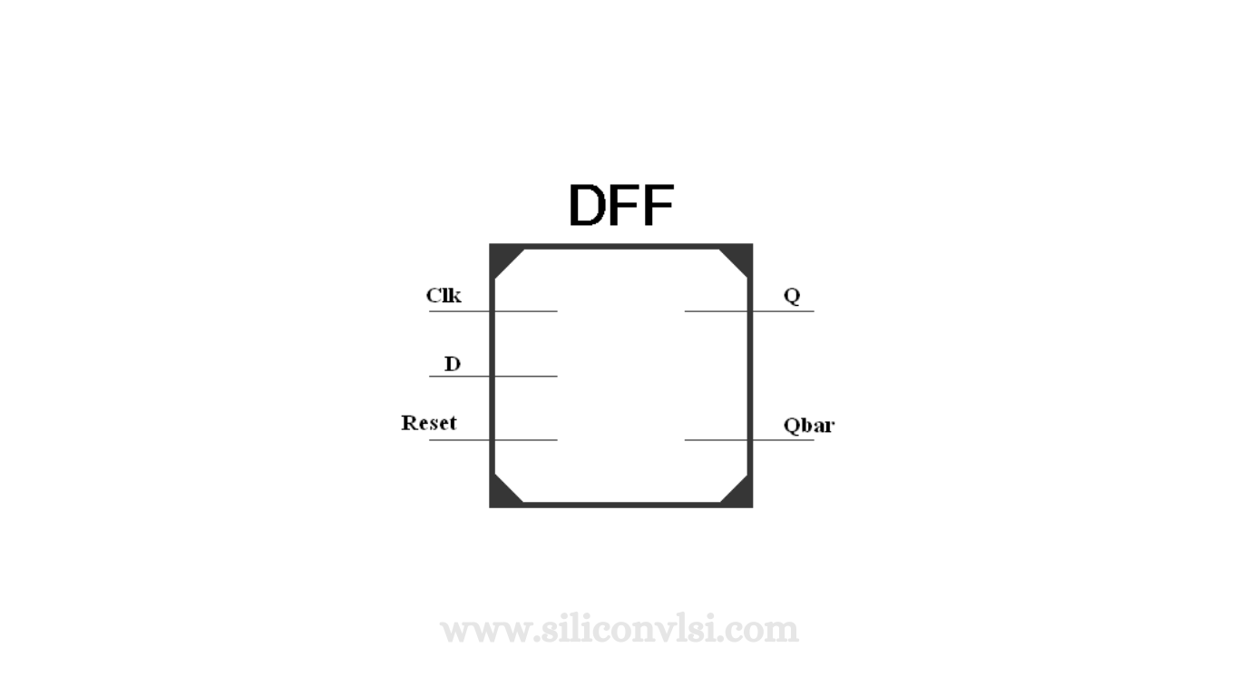
Figure 3 displays the Verilog module of a D Flip-Flop. The module takes a 1-bit input data line D. The control lines for the module consist of a 1-bit clock line Clk, which is provided by the 50 MHz on-board clock generator, and a 1-bit active-high reset. The output lines are Q and Qbar (the complement of Q). The output line Q takes on the same value as the input line D during the rising edge of the clock line Clk, provided that the reset line is low.
Verilog Code for Synchronous D Flip-Flop (DFF.v)
module DFF( Q,
Qbar,
D,
Clk,
Reset
);
output reg Q;
output Qbar;
input D,
Clk,
Reset;
assign Qbar = ~Q;
always @(posedge Clk)
begin
if (Reset == 1’b1) //If not at reset
Q = 1’b0;
else
Q = D;
end.
endmodule
Verilog Test Bench for Synchronous D Flip-Flop (DFF_tb.v)
`timescale 1ns / 1ps
module DFF_tb;
// Inputs
reg D;
reg Clk;
reg Reset;
// Outputs
wire Q;
wire Qbar;
// Instantiate the Unit Under Test (UUT)
DFF uut (
.Q(Q),
.Qbar(Qbar),
.D(D),
.Clk(Clk),
.Reset(Reset)
);
initial begin
// Initialize Inputs
D = 1’b0;
Clk = 1’b0;
Reset = 1’b1;
// Wait 100 ns for global reset to finish
#100;
// Add stimulus here
Reset = 1’b0;
#20;
forever #40 D = ~ D;
end
always #10 Clk = ~Clk;
endmodule
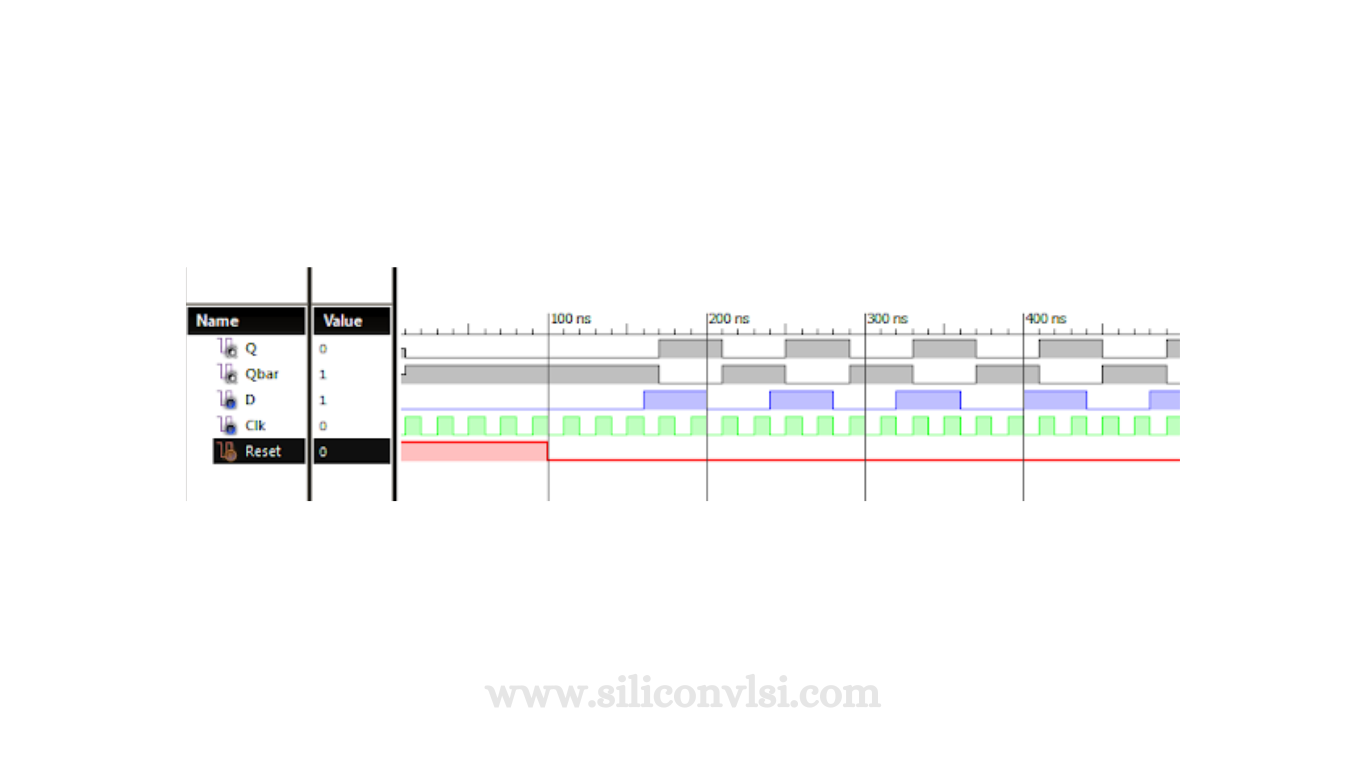
Timing Diagram of a D Flip-Flop
The following figure showcases the timing diagram of a synchronous D Flip-Flop.
Please note that the image references (like “Figure 1” or “Figure 2”) in the text above need to be replaced with the actual image links for the respective figures for accurate representation.