
Design of Two-stage OPAMP
Let’s discuss the construction of a simple two-stage operational amplifier (op-amp) and the advantages of using a pMOS differential amplifier with an nMOS common source stage for low-noise operation.
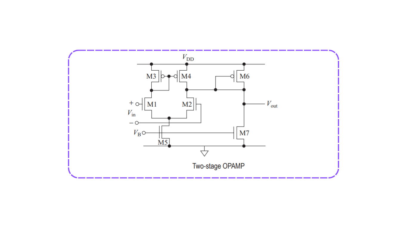
Construction of a Two-Stage Op-Amp
A basic two-stage op-amp can be built using the following configuration, as depicted in Figure 5.34:
Differential Amplifier: The op-amp begins with a differential amplifier stage. In this stage, two n-channel MOS transistors are often used, typically operating in saturation mode. This stage is responsible for amplifying the difference between two input signals.
Current Load: Following the differential amplifier, there is a common source stage with a constant current load. This stage helps maintain a stable bias current and improves the overall performance of the op-amp.
Current Source: The current source for the differential amplifier is usually implemented using an n-channel MOS transistor operating in saturation mode. It ensures a constant current flows through the differential amplifier.
Advantages of Two-Stage Op-Amp
The two-stage design offers several advantages:
Output Stage Optimization: With a two-stage structure, designers can optimize the output stage specifically for driving the load. This ensures that the op-amp can deliver the required output current with low distortion.
Input Stage Optimization: The first stage, which is the differential amplifier, can be tailored to provide good differential gain and common-mode rejection ratio (CMRR). This is crucial for accurate signal amplification and noise rejection.
Preference for pMOS Differential Amplifier with nMOS Common Source Stage
While Figure 5.34 illustrates a differential amplifier with nMOS transistors and an output stage with a pMOS driver, it’s noted that a pMOS differential amplifier combined with an nMOS common source stage is often preferred for applications requiring low noise operation.
This preference is due to the characteristics of pMOS transistors, which can offer lower noise performance compared to nMOS transistors. By using a pMOS differential amplifier in the input stage, noise levels can be reduced, making it suitable for applications where noise sensitivity is critical, such as high-precision analog circuits.
In summary, a two-stage op-amp is a common configuration that combines a differential amplifier with a common source stage. While Figure 5.34 depicts an nMOS-based differential amplifier with a pMOS output stage, for low noise applications, a pMOS differential amplifier with an nMOS common source stage is often preferred to minimize noise levels.