
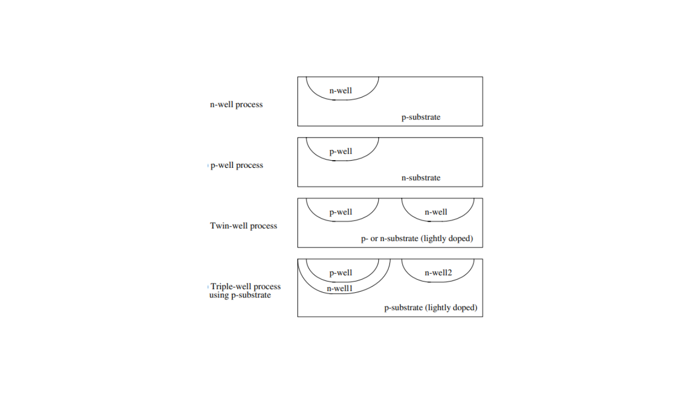
well Fabrication
In semiconductor manufacturing, we have NMOS (n-channel metal-oxide-semiconductor) and PMOS (p-channel metal-oxide-semiconductor) transistors. These transistors have different types of bodies: NMOS has a p-type body, while PMOS has an n-type body.
There are different ways to create these bodies, and the method used impacts the quality and performance of the transistors.
n-Well Process
In this process, NMOS transistors are made directly in the p-type substrate, while PMOS transistors are created in an n-well. An n-well is like a specific area within the substrate where the n-type material is dominant.
p-Well Process
Here, NMOS devices are formed in a p-well, and PMOS transistors are built in the n-type substrate. A p-well is like an isolated area where p-type material is prevalent.
Twin-Well Process
To mitigate excessive doping effects caused by counter-doping the substrate when making n-wells, a twin-well process is used. It involves using a substrate with lighter doping and creating both n-wells and p-wells. This reduces the need for heavy counter-doping.
Triple-Well Process
In situations where you want the bodies of MOSFETs (NMOS and PMOS) to be at different potentials, a triple-well process can be employed. An added n-well isolates the p-well from the substrate, allowing for different potentials. This helps in electrical isolation. In summary, these processes determine how NMOS and PMOS transistors are created within a semiconductor, affecting their performance and how they can be used in electronic devices.
What is the key distinction between the n-well process and the p-well process in semiconductor fabrication?
In the n-well process, NMOS transistors are fabricated in a p-type substrate, and PMOS transistors are created in the n-well. In contrast, the p-well process involves NMOS transistors in a p-well and PMOS transistors in an n-type substrate.
Why is counter-doping necessary when implanting the n-well in semiconductor fabrication?
Counter-doping is required to change the p-substrate’s concentration from p-type to n-type when creating an n-well. This is achieved by adding n-type dopants like phosphorous or arsenic.
What are the adverse effects of counter-doping the p-substrate to create an n-well, and why is it not as favorable as using intrinsic silicon?
Counter-doping can lead to excessive doping effects, causing acceptor atoms in the p-substrate to become ionized. This effect increases scattering and reduces mobility, negatively impacting semiconductor quality. Using intrinsic silicon and adding donor atoms is preferred.
How does the choice of substrate and the well process impact the quality and performance of PMOS devices?
PMOS devices fabricated in an n-well (n-well process) may suffer from excessive doping effects, resulting in reduced device quality and performance compared to PMOS devices created in a p-well (p-well process) or an n-substrate. For example, a PMOS device in an n-well can be slower than one in an n-substrate.