
What are the ESD models?
There are several types of ESD (Electrostatic Discharge) models including charged device model (CDM), machine model (MM), and human body model (HBM). In these, the HBM is most commonly used to test.
Human Body Model (HBM)
The Human Body Model (HBM) represents an ESD event caused by a charged human discharging the current into a grounded IC. HBM is the oldest and most common form of ESD. It really represents the discharge from the human body or any charged device into an ESD-sensitive device. When people walk, they generate some electricity and discharge it to the ground. Every step builds up a charge, This is also part of HBM.
The HBM testing model represents the discharge from the fingertip of a standing individual delivered to the device. It is modeled by a 100 pF capacitor, which is charged by a high-voltage supply through a high-ohmic resistor.

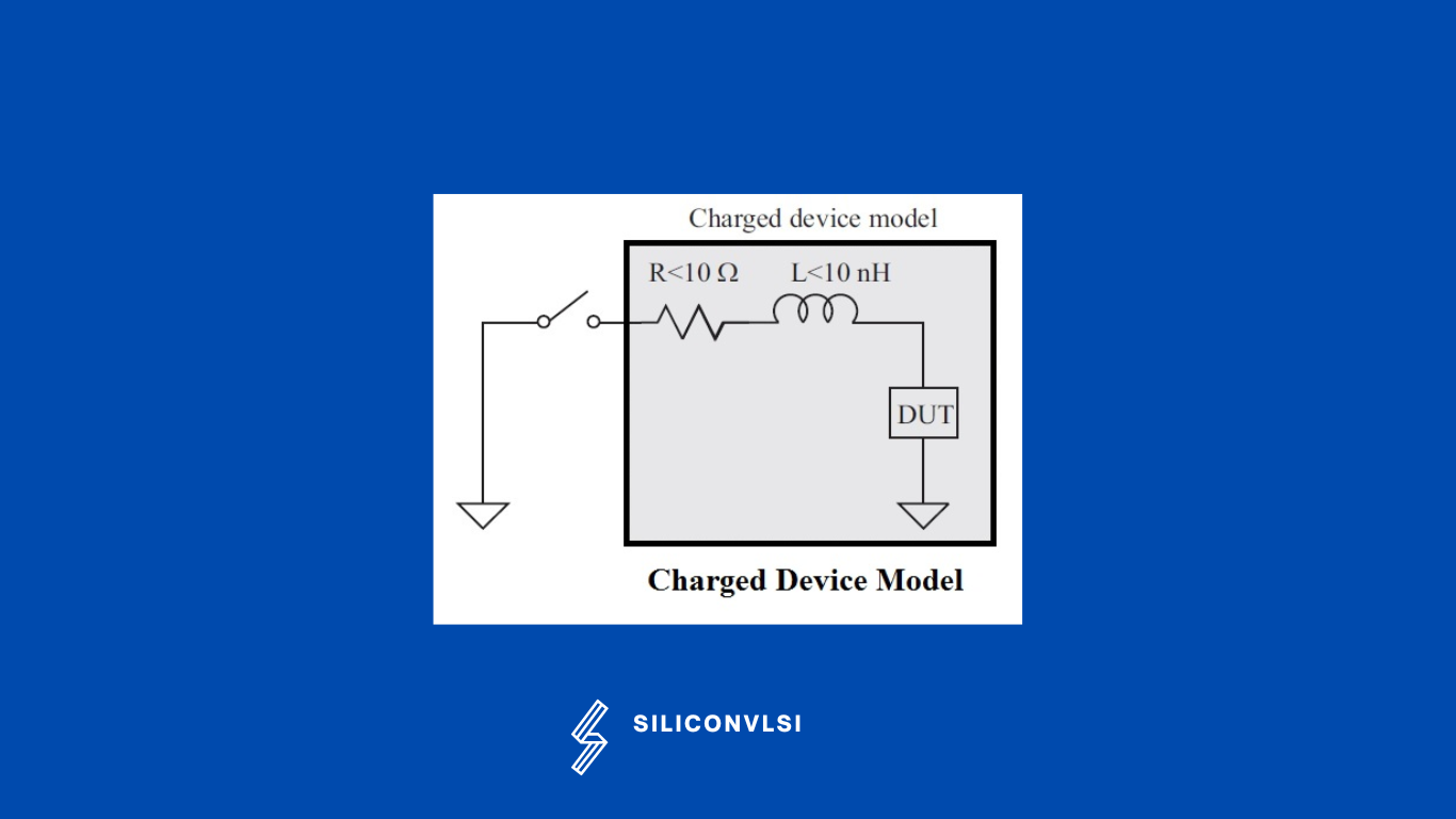
Charge Device Model (CDM)
The Charge Device Model (CDM) covers the ESD discharge when a device or an IC is self-charged during the manufacturing process and comes into contact with grounded equipment. If any device is sliding down the part feeder in automated handling equipment and then contacts the insertion head or another conductive surface, which is at a lower potential, a rapid discharge may occur from the device to the conductive surface. This discharge event is known as the Charged Device Model (CDM).
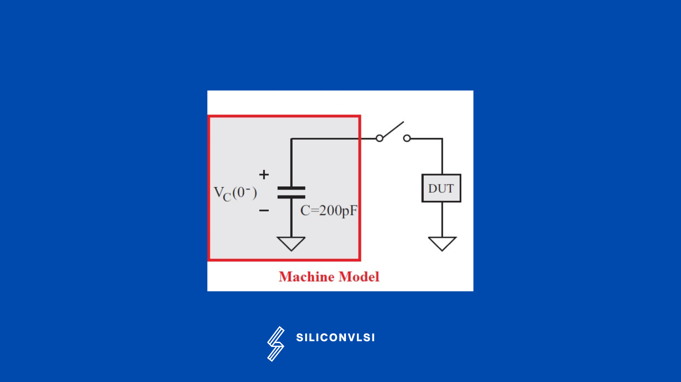
Machine Model (MM)
In Machine Model, a discharge can occur from an isolated conductor, or a charged conductive object, such as a metallic tool, or a piece of automatic equipment. Machine Model (MM) Component Level is similar in procedure to HBM testing. The basic test equipment and the stress combinations are the same, but the test head is very different.
ESD Protection Devices
- N-Well Resistors
- ESD Diode in CMOS
- Medium Voltage Triggered SCR
- Silicon Controlled Rectifiers (SCR)
- Gate-Coupled nMOS Transistors (GCNMOS)
- Gate-Grounded nMOS Transistors (GGNMOS)
ESD protection mechanism
- Thermal Breakdown of nMOS
- Avalanche Breakdown of nMOS
- Avalanche Multiplication in PN-junctions
- Current Limiting Characteristics of n-well Resistors
- ESD protection circuits as mentioned for a different model