
The snapback phenomenon in NMOS devices is an important aspect of understanding their behavior and reliability. It is closely connected to impact ionization and substrate current, which play significant roles in the breakdown of these devices. Let’s delve into this phenomenon, its contributing factors, and its implications in circuit design and electrostatic discharge (ESD) protection.
Snapback Phenomenon and Impact Ionization
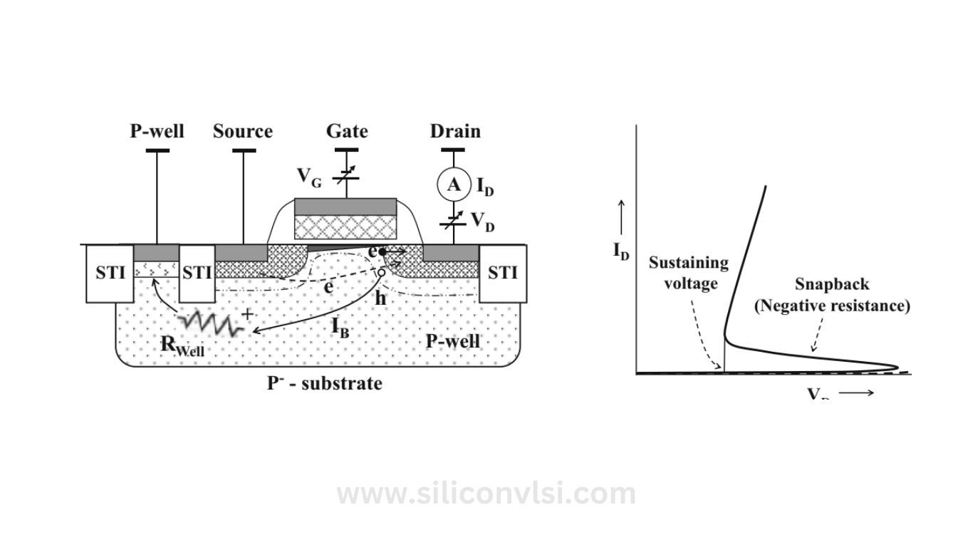
The snapback phenomenon is observed in NMOS devices when inversion carriers, i.e., electrons in the channel, gain sufficient kinetic energy to create secondary electron-hole pairs through impact ionization. This process results in an increased substrate current, which can have undesirable consequences for device performance and reliability.
In longer-channel NMOS devices, impact ionization mainly occurs near the drain, where the electric field is at its peak. However, as the channel length is reduced, the lateral electric field becomes stronger. This causes inversion carriers to reach the drain region with higher energy than in longer channels, leading to increased impact ionization and consequently higher substrate current.
Positive Feedback Loop and Negative Resistance
The excess substrate current resulting from impact ionization at the drain causes a rise in voltage drop across the well resistance (Rwell) underneath the source. This, in turn, locally forward biases the source-to-bulk junction. A portion of the injected electrons diffuses toward the drain, where they are subjected to impact ionization, further amplifying the carrier multiplication.
The increased hole current adds to the local forward voltage, leading to even higher injection at the source and creating a regenerative positive feedback loop. This loop is responsible for the observed negative resistance and snapback behavior in NMOS devices. The bipolar gain initially rises with the source-drain current, contributing to the negative resistance.
Implications and Design Considerations
In practical circuit design, it’s vital to consider the snapback phenomenon to ensure proper device operation and reliability. NMOS devices must be designed with a sustaining voltage higher than the maximum operating voltage. Achieving this involves optimizing the doping profile and NMOS layout to increase the snapback voltage, thereby preventing interference with CMOS operation.
For instance, a higher retrograde P-well concentration reduces the substrate resistance and elevates the current level at which snapback initiates. Employing a longer channel length and introducing silicide can decrease the bipolar gain, leading to a higher snapback voltage. Additionally, aligning the source and substrate contacts helps minimize the good resistance.
ESD Protection and Snapback
Understanding the snapback mechanism is Important for utilizing NMOS devices for protection against electrostatic discharge (ESD). When subjected to ESD events, the snapback phenomenon can help divert excessive current away from sensitive components, safeguarding the circuitry. By exploiting the snapback behavior, NMOS devices can efficiently shunt ESD-induced currents to protect the rest of the circuit.
In conclusion, the snapback phenomenon in NMOS devices arises from impact ionization and secondary carrier generation. It leads to a regenerative positive feedback loop, resulting in negative resistance and snapback behavior. This phenomenon has important implications for circuit design, requiring careful consideration of sustaining voltage and layout optimization. Furthermore, the snapback behavior can be harnessed for ESD protection, making it a valuable aspect of semiconductor device engineering.