
Silicon Crystalline Orientation
In the world of VLSI, we often talk about how scaling transistors impacts carrier mobility. Over time, as transistors have shrunk, the effective mobility of carriers in the channel has significantly reduced. I’ve learned that this is largely because we increase channel doping to control short-channel effects, which unfortunately also introduces more charged impurities. These impurities scatter the carriers and reduce their mobility, making transistors slower.
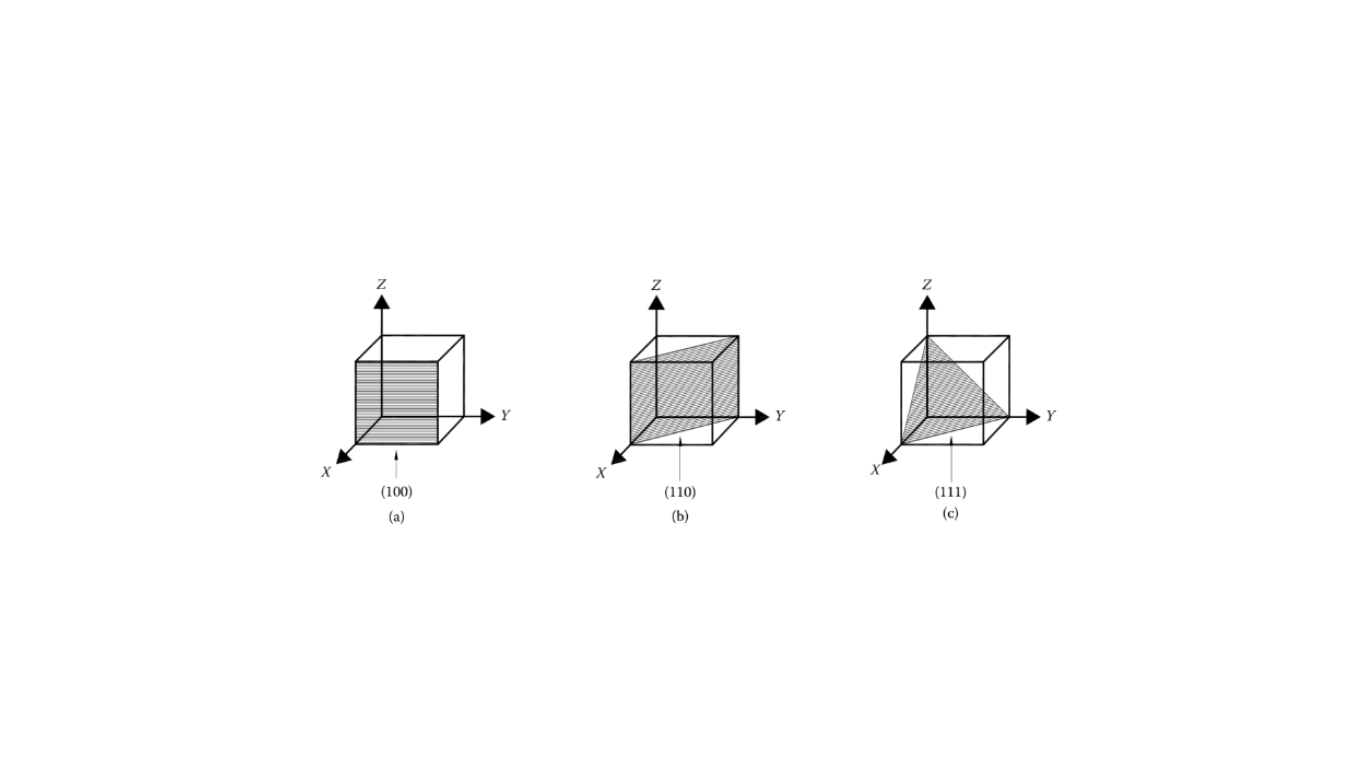
How does crystalline orientation affect transistors?
But there’s more to this story when we consider the crystalline orientation of silicon substrates. You might already know that for years, we’ve been using (100) silicon wafers in CMOS fabrication. Why? Well, it’s because this orientation gives us high electron mobility, which is great for nMOS transistors, along with a low interface trap density. However, I’ve come across a trade-off here: pMOS transistors don’t perform as well on (100) wafers due to lower hole mobility.
What are the benefits of a (110) silicon wafer?
Now, you might wonder why we don’t just switch to a better option for pMOS. The good news is that we can. By using a (110) silicon orientation, we can improve hole mobility by up to 30%, significantly boosting pMOS performance. Of course, this comes with a slight downside: the electron mobility for nMOS decreases by about 5–10%.
How does hybrid-orientation technology balance nMOS and pMOS performance?
Here’s where it gets interesting: we can optimize both nMOS and pMOS performance with something called hybrid-orientation technology. In this approach, we use (100) wafers for nMOS transistors and (110) wafers for pMOS. It’s like getting the best of both worlds, improving performance without severely compromising either transistor type.
How can we improve pMOS performance with simple wafer alignment?
There’s also a simple, cost-effective solution for enhancing pMOS performance on (100) wafers. By rotating the wafer flat or notch to align the channel direction along the <100> direction, we can increase pMOS mobility by around 15%, all without significantly affecting nMOS performance. It’s a clever trick that’s already being used in high-volume production since the 120nm technology node.
Finding the balance between electron and hole mobility
In summary, when we talk about silicon wafer orientation, it’s all about finding the right balance between electron and hole mobility. Whether it’s (100) for nMOS or (110) for pMOS, the choice we make can have a huge impact on the overall performance of a chip. Understanding these differences helps us make better decisions in design and manufacturing.
1 Comment
I do agree with all the ideas you have introduced on your post They are very convincing and will definitely work Still the posts are very short for newbies May just you please prolong them a little from subsequent time Thank you for the post