
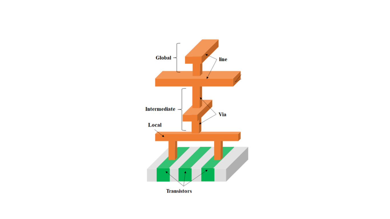
Interconnect variations
Interconnect variations in semiconductor chips can lead to variations in interconnect capacitance and resistance, which, in turn, affect the performance of clock distribution networks. These variations are primarily caused by both vertical and lateral dimensions and can result in clock skew. Here are the key factors contributing to interconnect variations:
Inter-level Dielectric (ILD) Thickness Variations
In the formation of aluminum interconnect, silicon dioxide layers are deposited between layers of patterned metallization. Chemical-mechanical polishing (CMP) is used to planarize the surface and remove topography resulting from the deposition and etching processes. While CMP can achieve good planarity at a local scale (over individual metal lines), it faces limitations in achieving global planarization. Variations in polish rates occur due to layout density and pattern effects. Higher polish rates in lower spatial density regions result in smaller dielectric thickness and higher capacitance. Analytical models have been developed to estimate ILD thickness variations based on spatial density, making it possible to correct systematic components during the design phase by adding appropriate delays or uniformizing density using “dummy fills.” Clock distribution networks can benefit from this information to reduce clock skew by considering the dielectric thickness variations.
Deviation in Wire Width and Line Spacing
Variations in the width of wires and line spacing also contribute to interconnect variations. These variations are influenced by photolithography and etch dependencies. At lower levels of metallization, lithographic effects are significant, while etch effects become more important at higher levels. Wire width directly impacts resistance, while line spacing affects wire-to-wire capacitance, which is a dominant component of capacitance in interconnect networks. Interconnect variations are a critical consideration in semiconductor process development and manufacturing. They can lead to clock skew and affect the performance of clock distribution networks. Understanding and controlling these variations are essential for optimizing chip performance and ensuring reliable operation.
What are the main causes of skew in clock distribution within an integrated circuit?
Skew in clock distribution is mainly caused by static variations in interconnect capacitance and resistance across a chip. These variations, particularly in inter-level dielectric (ILD) thickness, lead to differences in signal propagation delays.
How is chemical-mechanical polishing (CMP) used in semiconductor manufacturing, and what challenges does it pose for achieving planarity?
CMP is used to planarize the surface of semiconductor wafers by removing topography resulting from deposition and etching processes. While CMP can achieve excellent planarity at the feature scale, challenges arise when trying to achieve global planarization due to variations in polish rate, which are influenced by circuit layout density and pattern effects.
How do variations in wire width and line spacing impact interconnect performance?
Variations in wire width and line spacing can affect interconnect performance. These variations result from photolithography and etch dependencies. Photolithographic effects become more critical at lower levels of metallization, while etch effects, which depend on width and layout, become important at higher levels. Wire width affects resistance, while line spacing impacts wire-to-wire capacitance, which is a dominant component of capacitance.