
Junction-Isolated Transistors
Early planar transistor technology utilized reverse-biased pn junctions to provide isolation between components. One of the earliest versions of junction-isolated transistors was the triple-diffused process, involving three ion implantations and subsequent diffusion. However, this process led to a significant collector resistance issue and lower npn performance.
The most common junction-isolated transistor is the buried-collector process. It builds upon the concepts shown earlier but includes an n+-collector plug and isolation created by diffused p+ regions surrounding the transistor. The diffusion of base and emitter impurities into the epilayer allows better control of the base width. However, junction-isolated transistors have drawbacks, including larger chip area requirements and limitations on high-speed operation due to parasitic capacitances and deep diffusions.
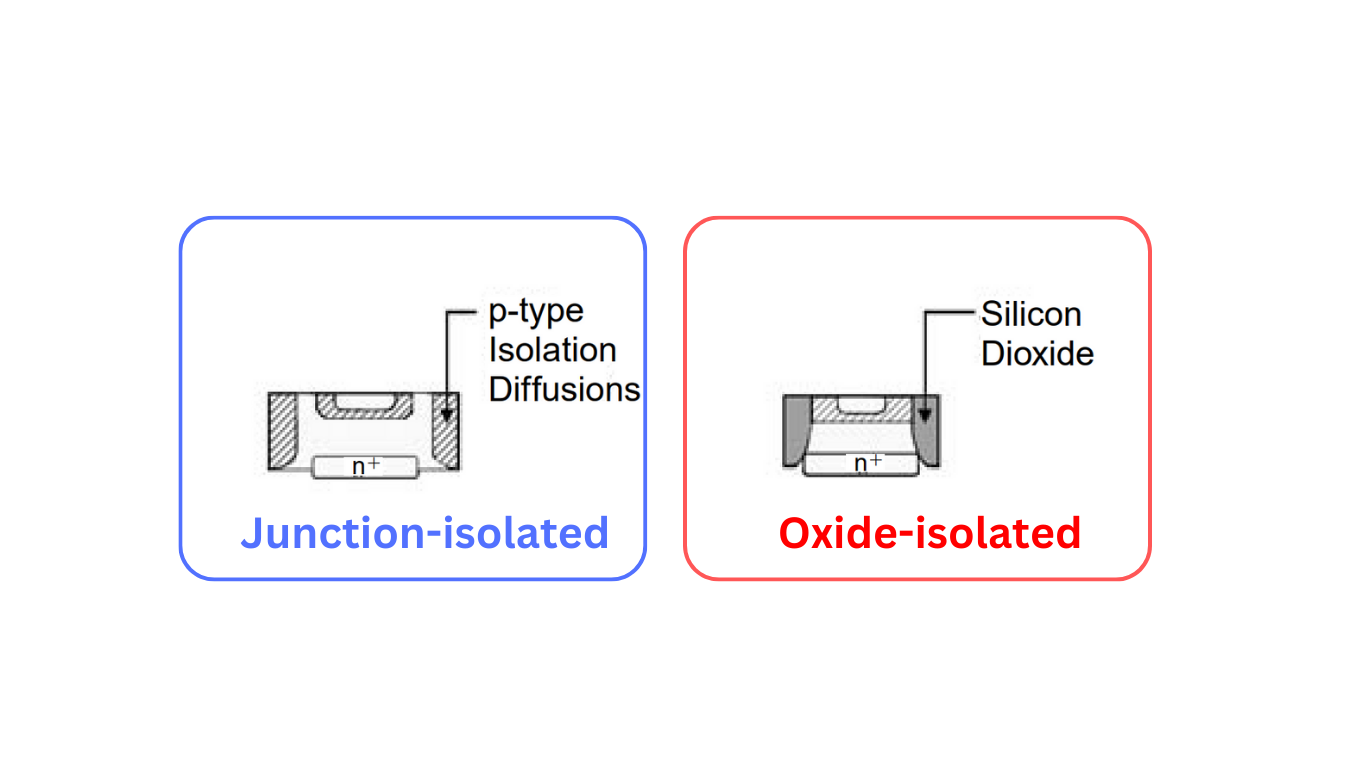
Oxide isolation offers significant advantages, reducing both lateral and vertical dimensions of buried-layer collector transistors. This reduction is possible because base and collector contacts can extend to the edge of the isolation region. Additionally, the emitter can be walled against the oxide edge, saving the chip area.
The principal difference between scaling junction- and oxide-isolated transistors is illustrated in Figure. Oxide-isolated transistors can have their base and collector contacts extended over the collector region. This difference allows for more compact designs.
The process flow for an oxide-isolated bipolar transistor of the buried-layer collector type involves several steps, including subcollector formation, epitaxial growth, device isolation, base formation, emitter/base contact mask patterning, emitter implantation, and contact formation. The result is a transistor with reduced isolation capacitance, thinner epitaxial layers, and shallower emitter/base diffusions. These features contribute to higher-speed operation, with typical fT values ranging from 1 to 10 GHz. However, further speed enhancement is challenging due to parasitic capacitances and resistances from contact areas and alignment tolerances.
What are the main disadvantages of junction-isolated transistors?
Junction-isolated transistors occupy a relatively large chip area due to the isolation region, making them unsuitable for VLSI applications. Additionally, they have limitations in high-speed operation due to large parasitic capacitances and deep diffusions.
What advantages does oxide isolation offer over junction isolation in terms of transistor performance?
Oxide isolation reduces isolation capacitances, allows for thinner epitaxial layers, and results in shallower emitter/base diffusions. These factors contribute to higher transistor performance, with an fT typically in the range of 1–10 GHz.