
Matching Concepts for Capacitor
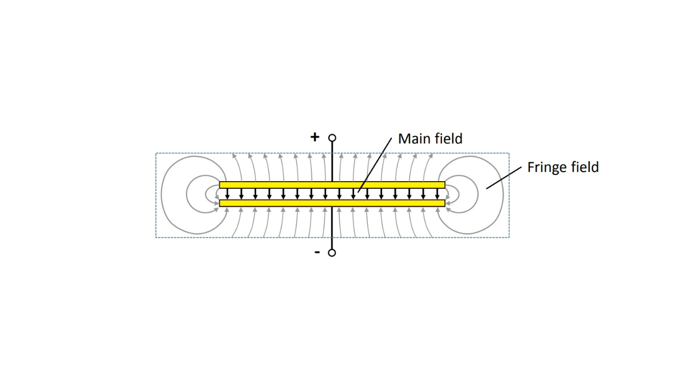
When designing capacitors in integrated circuits, it’s crucial to consider the impact of fringe fields on capacitance. While the ideal parallel-plate capacitor’s capacitance can be calculated using a basic equation, this calculation only accounts for the proportion of capacitance generated by the homogeneous field between the plates. Fringe fields, which exist outside the main field, contribute significantly to capacitance but are not considered in the ideal equation.
Fringe Effects on Capacitors
- An ideal parallel-plate capacitor’s capacitance is calculated using a formula that applies to the homogeneous field between the plates.
- However, fringe fields outside this main field contribute to capacitance, and these fringe effects are not considered in the ideal formula.
- Designing capacitors that closely resemble ideal parallel-plate capacitors minimizes fringe effects, ensuring accurate capacitance matching.
Layout Design for Matching Capacitors
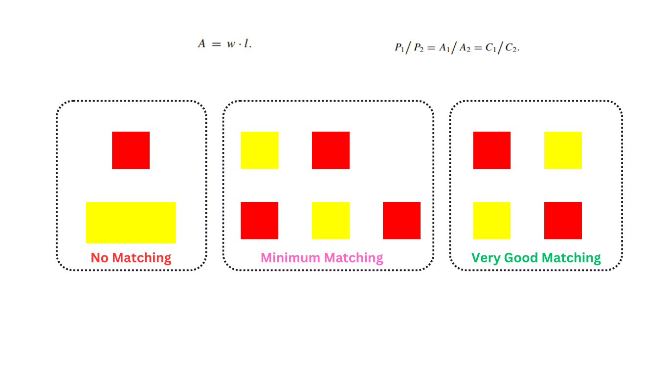
- Matching capacitors aim for uniform capacitance values despite manufacturing tolerances affecting layout parameters.
- The width (w) and length (l) of capacitors are subject to manufacturing tolerances, leading to fringe effects.
- Capacitors with symmetric and compact layouts are preferred for matching, as they minimize fringe effects.
- The ratio of perimeter (P) to surface area (A) is crucial for accurate matching.
Two Matching Approaches
- First Approach – Splitting Capacitors:
- Capacitors are divided into identical single capacitors connected in parallel.
- These single capacitors are symmetrical, ensuring that fringe fields and main fields are in proportion, leading to matching.
- Fringe effects due to fabrication tolerances affect all single capacitors equally, resulting in no mismatch.
- Second Approach – Individual Stretching:
- Above Equation is used to define the dimensions of two rectangular capacitors.
- Quadratic capacitors (w = l) are preferred as the “quadratic candidate.”
- Quadratic equations are solved for the dimensions of the second capacitor based on the desired capacitance ratio.
- This approach minimizes the P/A ratio.
- However, it is suitable only when the capacitances of matching capacitors do not differ significantly.
- High-precision matching may not be achievable with this method due to fabrication tolerance effects that increase with the C2:C1 ratio.
Considerations
- The aspect ratio (l/w) for capacitors designed using the second approach may become unfavorable for larger C2:C1 ratios.
- Fabrication tolerances impact dimensions differently, leading to unavoidable remaining mismatches with the stretching method.
- High-precision matching capacitors are best achieved through the first approach of splitting capacitors.
Matching capacitors accurately is essential in analog circuit design to maintain consistent performance and reduce the impact of fringe effects caused by manufacturing tolerances and layout variations.