
Matching Devices
Location-dependent variations in parameter settings across a wafer are a common issue in semiconductor manufacturing. These variations result from tolerances in the fabrication process and can significantly affect the electrical properties of devices on the wafer
Location-Dependent Variations
- Variations in device parameters across the wafer are caused by fabrication tolerances and affect the electrical properties of devices.
- These parameter variations are often unknown because fabrication tolerances are stochastic, leading to uncertainties.
The Challenge of Uncertainties
- Dealing with these uncertainties is a challenge in analog circuit design, as the parameters influencing them are typically not precisely known.
The Importance of Device Placement
- To address this challenge, a key matching concept is to place matching devices as close as possible to each other in the layout.
- The smaller the layout distance between matched devices, the less impact unknown gradients, regardless of their origin or magnitude, can have on creating mismatches.
The Impact of Device Placement
- An example illustrates the significance of device placement:
- Two MOS-FETs are to be matched in a 2:1 ratio.
- When these devices are placed far apart (several millimeters), the matching quality is poor because parameter settings, such as the Nwell sheet resistance, affect them differently due to the large separation.
- Placing devices at a minimal distance (in the µm scale) improves matching significantly.
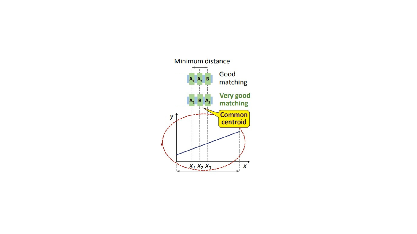
Enhancing Matching Through Subdevice Splitting
- Matching can be further improved by splitting devices into subdevices and interdigitating them between each other.
- This arrangement brings the focal points of the devices closer together and reduces the effective distance between them.
- Subdevice splitting and interdigitation enhance matching precision.
In summary, matching devices closely in the layout is a fundamental concept to mitigate the impact of location-dependent variations in parameter settings, ensuring better-matching quality in analog circuit design.