Close Menu
  • Analog Design
    • Latest Analog Layout Interview Questions (2025)
  • Digital Design
    • Digital Electronics Interview Question(2025)
    • Top VLSI Interview Questions
  • Physical Design
    • Physical Design Interview Questions for VLSI Engineers
  • Verilog
    • Verilog Interview Questions(2024)
  • Forum
Facebook Instagram YouTube LinkedIn WhatsApp
SiliconvlsiSiliconvlsi
Forum Questions Register in Forum Login in Forum
Facebook Instagram YouTube LinkedIn WhatsApp
  • Analog Design
    • Latest Analog Layout Interview Questions (2025)
  • Digital Design
    • Digital Electronics Interview Question(2025)
    • Top VLSI Interview Questions
  • Physical Design
    • Physical Design Interview Questions for VLSI Engineers
  • Verilog
    • Verilog Interview Questions(2024)
  • Forum
SiliconvlsiSiliconvlsi
Home»Analog Design»How to solve NWELL Antenna Effect
Analog Design

How to solve NWELL Antenna Effect

siliconvlsiBy siliconvlsiJuly 19, 2022Updated:May 12, 2024No Comments1 Min Read
Facebook Pinterest LinkedIn Email WhatsApp
Share
Facebook Twitter LinkedIn Pinterest Email

What is Nwell Antenna Effect

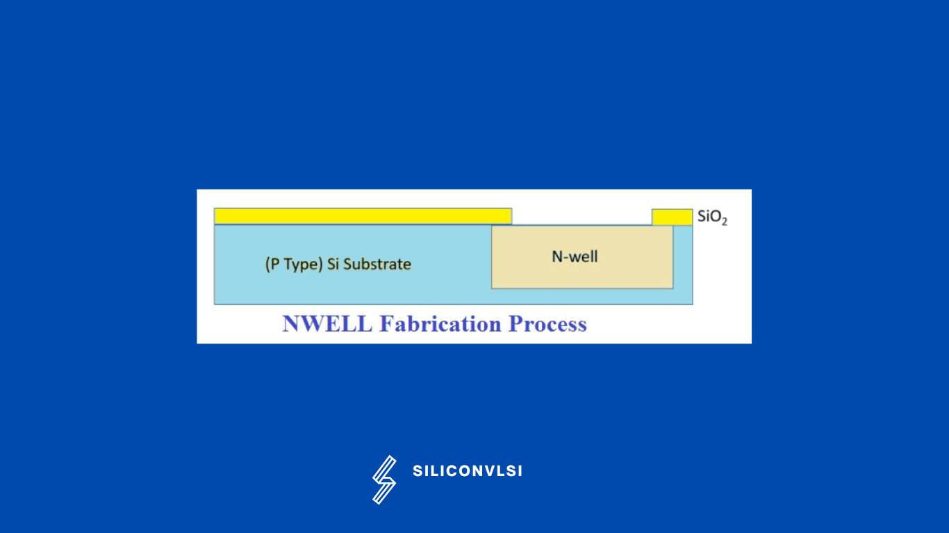
Nwell is fabricated by ion Implantation, During the fabrication process, some charges are accumulated on Nwell. The charge build-up may not be from the gate to the body in CMOS, but  It can also be the body(nwell) to the gate of a MOSFET. So we can say that during fabrication, before contact and metal, there can be a charge build-up on the body of a pMOS transistor (nwell) relative to the gate. Now after nwell fabrication, the next step is gate(poly) fabrication for self-alignment purposes, now if the charge on nwell is huge, then it may, damage the gate oxide under the poly, this is called as nwell antenna Effect in VLSI.

NWELL Antenna Effect

How to Solve Nwell Antenna Effect

  • We should put N+(bulk connection) to Nwell.
  • The N+/P diode should provide enough leakage to prevent any damage to the gate oxide.


Share. Facebook Twitter Pinterest LinkedIn Tumblr Email

Related Posts

BJTs vs. MOSFETs: Key Differences Every Analog Designer Should Know

April 3, 2025

Understanding the 2.5D Approach in Packaging Technology

December 1, 2024

Essential Analog Layout Interview Questions: Unveiling Key Insights

August 3, 2024
Leave A Reply Cancel Reply

Facebook X (Twitter) Instagram Pinterest Vimeo YouTube
  • About Us
  • Contact Us
  • Privacy Policy
© 2025 Siliconvlsi.

Type above and press Enter to search. Press Esc to cancel.