
Matching Concepts for Orientation-Dependent Effects
In semiconductor device design, achieving precise device matching is crucial for reliable circuit performance. To ensure effective matching, especially in the case of resistors and other devices, specific alignment considerations must be taken into account:
Alignment Tolerances
The same Orientat device matches well.
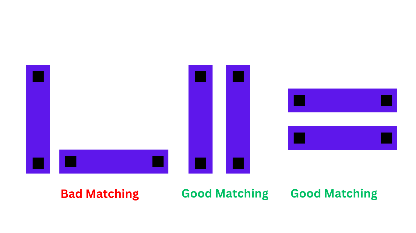
Alignment tolerances are inevitable during the semiconductor fabrication process.
To minimize the impact of alignment tolerances on device matching, it’s recommended to align all matching elements in the same direction.
For example, in the case of resistor contacts, misalignment can affect resistor heads differently based on orientation. Aligning resistors in parallel ensures consistent matching even with alignment shifts.
2. Carrier Mobility:
Mechanical forces can influence charge carrier mobility, particularly related to crystal lattice alignment.
Similar to alignment tolerances, aligning all elements in a matching group uniformly ensures that mechanical forces impact them in the same way, reducing mismatches.
3. Thermoelectric Effect:
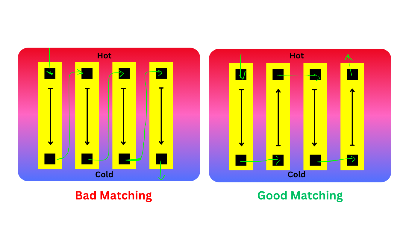
The thermoelectric effect results in potential differences at contact surfaces between different materials. This effect can cause voltage variations at interfaces.
These voltage differences depend on temperature and material-specific Seebeck coefficients, and they don’t cancel out when contact boundaries are at different temperatures.
For instance, metal-silicon contacts can be significant. To offset Seebeck voltages, it’s essential to ensure that currents flow in both directions in split devices as much as possible.
In cases where complete offsetting is challenging, it’s advisable to make sure that currents in matched devices flow in the same direction.
4. Avoiding Geometric Symmetry Axes:
Layout designers should be cautious when relying solely on the geometric symmetry axis to achieve symmetry in the current flow.
Geometric symmetry axes can inadvertently mirror currents in associated devices, which can lead to mismatches.
To prevent this, designers should consider the direction of the current flow explicitly.
In summary, when designing semiconductor devices for matching, alignment plays a critical role. By aligning matching elements in the same direction, taking into account carrier mobility effects, and managing thermoelectric effects, designers can minimize mismatches and ensure reliable circuit operation.