
Programmable Logic Device
Programmable logic devices (PLDs) are standard products that can be programmed to obtain the desired functionality. An IC that contains large numbers of gates, flip-flops, etc. that can be configured by the user to perform different functions is called a Programmable Logic Device (PLD).PLDs are less board space, faster, lower power requirements, less costly assembly processes, higher reliability, and availability of design software.
The PLDs which are programmed by the manufacturer are known as Mask-Programmable Logic Devices. The PLDs, which are programmed by the end user are called Field-Programmable Logic Devices (FPLD). The architecture of PLDs is very regular and fixed. It cannot be changed by the end user.
The PLDs have a wide range of applications and have low risk and cost in manufacturing in large volumes. Hence, the PLDs are cheaper. As the PLDs are premanufactured, tested, and placed in inventory in advance, the design cycle time is very short.
Programmable Logic Devices are classified into three categories:
- Read-only memory (ROM)
- Programmable logic array (PLA)
- Programmable array logic (PAL)
Read Only Memory
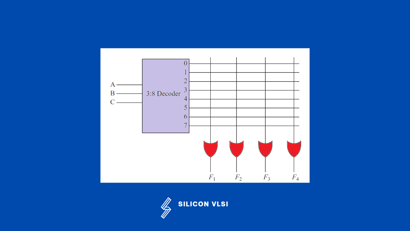
The memory from which we can only read but cannot write on, it called a Read-only memory (ROM). Read-only memory (ROM) is a memory chip that can be programmed once to store binary data. The simplest architecture of 8 × 4 ROM is shown in the following figure.
It has a decoder with k inputs and 2k output lines. The output lines of the decoder are connected to the inputs of OR gates with programmable interconnections. All the interconnections (in this case 32) are programmable. The interconnections have fuses that can be opened or blown by applying high-voltage pulses into the fuses. #
Types of ROM
- Erasable PROM (EPROM) #
- Electrically erasable PROM (EEPROM)
- Programmable read-only memory (PROM)
How does ROM work?
Similar to a disc array, ROM operates. To turn the system on and off, a grid of rows and columns is contained there. Each component of the array corresponds to a particular memory component on the ROM chip. The appropriate components are connected using a diode. #
Advantages of ROM
- It is easy to test. #
- Less expensive than RAM.
- Its static nature means it does not require refreshing.
Disadvantages of ROM
- ROM is its slow speed and inability to store large amounts of information. #
- After burning or programming a PROM chip, you cannot erase or change its data.
- If an MROM contains a design error, you cannot use it, and the code requires replacement.
Programmable Logic Array
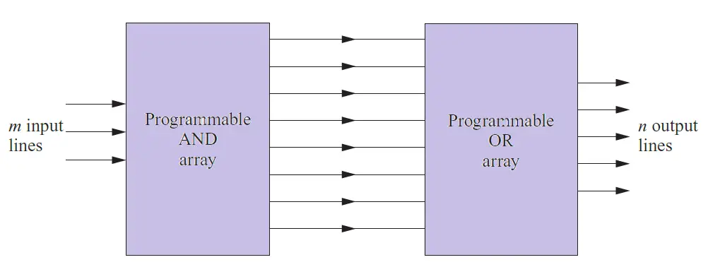
A programmable Logic Array is a type of PLD, which has both a programmable AND array and a programmable OR array. The AND array is programmed to generate the product terms and then ORed by programming the OR array. The structure of PLA is shown in the following figure. #
Programmable Array Logic
Programmable Array Logic and Programmable Logic Array are types of PLDs (programmable logic devices), and these are mainly used for designing combination logic mutually by sequential logic.
PAL also includes flip-flops so that they can be used to design state machines. The AND array is programmed to generate the product terms or literals of the Boolean functions to be implemented and then ORed by the OR plane to generate the functions.
Programmable array logic (PAL) is another programmable architecture that can be programmed to implement the desired function. The PAL architecture is shown in the following figure. It has a programmable AND array or plane followed by a fixed OR array or plane. #
Block diagram of PAL architecture
Advantages of Programmable Logic Devices
- Less design time. #
- Less power requirement.
- Low development cost.
- Less space requirement.
- High reliability.
- Easy design modification.
- It is easy to troubleshoot.
- High switching speed.
- High design security.
- Easy circuit testing.
Disadvantages of Programmable Logic Devices
- Lack of security. #
- Large power requirement.
- The high-cost solution in large quantities.
- It requires a large area and poor performance.
- Additional cost, power, space requirements, etc.