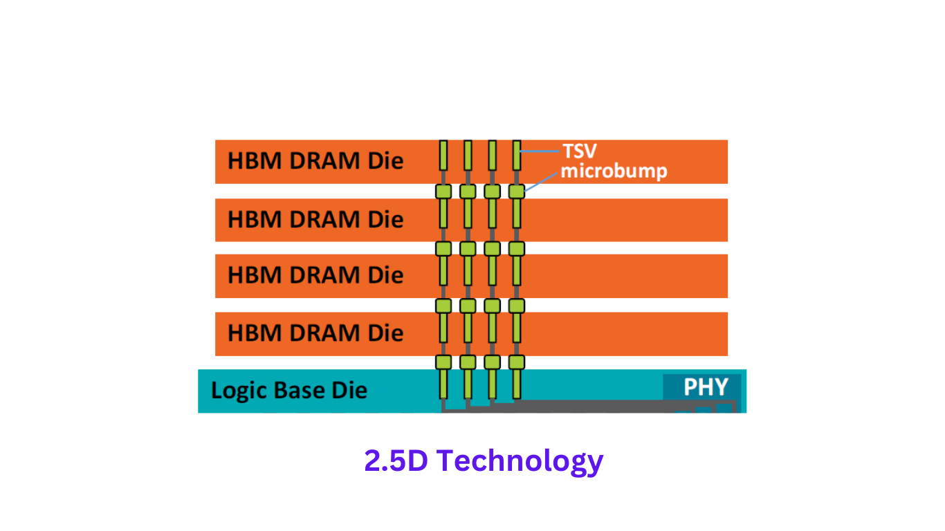
What is the 2.5D Approach?
The 2.5D approach in packaging technology represents a significant advancement in semiconductor packaging, bridging the gap between traditional 2D and more advanced 3D methods. Unlike 2D packaging, which generally demonstrates limitations in density and connectivity, the 2.5D method employs an innovative design strategy that incorporates an interposer separately from the active components, allowing for more efficient chip connectivity. The interposer serves as a medium that facilitates communication between multiple chips placed on a single substrate, significantly enhancing performance.

One of the essential features of the 2.5D approach is its ability to support heterogeneous integration. This means that various types of chips, including logic, memory, and analog devices from different manufacturers, can be interconnected within a single package. This capability promotes not only a higher chip density but also improved performance because the chips can operate together more efficiently due to the close proximity afforded by the interposer structure. Additionally, this approach enhances signal integrity as it minimizes the distance that signals must travel, which directly reduces latency and improves overall system performance.
Thermal management is another crucial aspect of the 2.5D packaging approach. With the chips mounted closer together and interconnected through the interposer, effective heat dissipation becomes imperative. Advanced materials and designs, including the use of embedded cooling solutions, can be implemented to manage the heat generated during operation, ensuring that the devices function optimally without overheating. Overall, the 2.5D approach marks a significant evolution in semiconductor packaging, combining the advantages of both 2D and 3D technologies to provide a more robust solution for modern electronic applications.
Advantages of the 2.5D Packaging Technology
The 2.5D packaging technology offers several advantages that position it favorably against traditional packaging methods. One of the primary benefits is its enhanced performance. By allowing multiple chips to be integrated on a single interposer, 2.5D packaging facilitates faster data transfer between components. This is essential for applications that require high bandwidth and rapid processing capabilities, particularly in fields such as telecommunications and data centers.
Another significant advantage of 2.5D technology is its ability to reduce power consumption. As devices become increasingly complex, managing power efficiency is critical. The interposer design in 2.5D packaging enables shorter electrical connections, which minimizes signal loss and could lead to overall lower operational power requirements. This reduction in power consumption not only improves the efficiency of the devices but also contributes to heat management, thereby enhancing thermal performance.
Thermal management is crucial for electronic devices, especially as they operate at higher speeds. The 2.5D approach supports improved thermal dissipation through its better-defined pathways for heat flow. This is achieved by distributing heat across the larger area of the interposer, allowing for more effective heat spreading and preventing potential overheating issues.
Moreover, the design flexibility offered by 2.5D packaging opens up new avenues for innovation. It allows engineers to combine different types of components with varying functionalities on the same substrate, leading to heterogeneous integration. This capability enhances the overall device functionality while adhering to strict spatial constraints, leading to compact designs without sacrificing performance. The result is a diverse mix of components that can significantly boost device capabilities, making 2.5D packaging a standout choice for modern electronics.
Future Trends and Applications of 2.5D Packaging
As the demand for more advanced electronic devices escalates, the 2.5D packaging technology is poised to play a pivotal role across various sectors, including consumer electronics, automotive, and artificial intelligence (AI) systems. This innovative approach allows for greater integration of multiple components within a compact space, which is essential for the miniaturization of electronic devices and enhancing performance. Key trends indicate a growing reliance on 2.5D packaging to address the increasing complexity of modern electronic designs.
In the consumer electronics sector, manufacturers are increasingly adopting 2.5D packaging to develop high-performing smartphones, tablets, and wearable devices. This technology enables the integration of multiple chiplets, which not only reduces size but also improves power efficiency and thermal management. As a result, we can expect a significant improvement in device capabilities without compromising performance or usability. Moreover, the rise of smart home devices and the Internet of Things (IoT) is expected to drive further innovation in 2.5D technology, providing enhanced connectivity and user experiences.
Read also: Difference Between SRAM and DRAM(Advantages of SRAM over DRAM)
In the automotive industry, the shift towards electric and autonomous vehicles presents a unique opportunity for 2.5D packaging. This technology can effectively manage the demanding semiconductor requirements necessary for advanced driver-assistance systems (ADAS) and other critical functionalities. The compact nature of 2.5D packaging allows for the integration of sensors, processors, and communication components, leading to improved safety and efficiency in automotive applications.
Furthermore, the integration of 2.5D packaging with System-in-Package (SiP) solutions and advanced chiplet architecture has opened the door for unprecedented research and development. This convergence enables agile manufacturing and design processes, fostering innovation across various fields. As research progresses, the interplay between 2.5D packaging and emerging technologies promises to revolutionize electronic design and production methodologies, ultimately impacting future electronic devices significantly.
1 Comment
Nice post. I learn something totally new and challenging on websites