
Verilog Code for 3-to-8 Decoder
A 3-to-8 decoder is an essential combinatorial logic device, featuring three input lines and eight output lines. Each unique combination of the three binary input lines results in a single output signal set to logic 1. This decoder acts as a min-term generator, where each output corresponds to a specific min-term. Due to its significance, decoders find extensive applications in the design of digital systems.
Decoder Input and Output
The input of a 3-to-8 decoder has a logarithm base 2 of ‘n,’ meaning it has three input lines (n=3). On the other hand, it possesses ‘n’ bits of output, which translates to eight output pins. Out of these eight pins, only one pin will have a value of 1, while the rest will be 0, providing a unique binary representation for each input combination.
Example: 3-to-8 Decoder
For a 3-to-8 decoder, the input is represented by three bits of a binary input number, and the output is a single bit that corresponds to the value of the binary input number being set to 1.
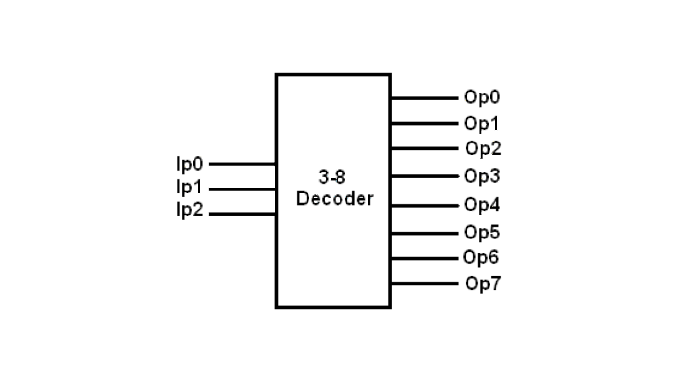
Block Diagram of a 3-to-8 Decoder
Below is the block diagram of a 3-to-8 decoder, giving a visual representation of its structure and functionality.
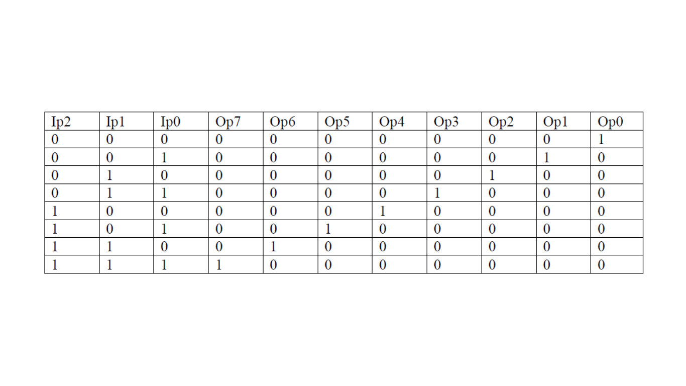
Truth Table for 3-to-8 Decoder
The truth table for a 3-to-8 decoder is shown below. It illustrates all possible combinations of the three input lines (Ip0 to Ip2) and their corresponding eight output lines (Op0 to Op7).
Verilog Module: Implementing the 3-to-8 Decoder
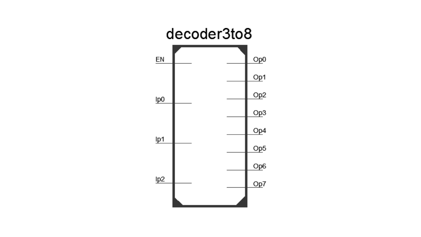
To understand the implementation of the 3-to-8 decoder in Verilog, refer to the Verilog module code provided below:
module decoder3to8(
input Ip0,
input Ip1,
input Ip2,
input EN,
output reg Op0=0,
output reg Op1=0,
output reg Op2=0,
output reg Op3=0,
output reg Op4=0,
output reg Op5=0,
output reg Op6=0,
output reg Op7=0
);

always @ (EN, Ip2, Ip1, Ip0)
begin
Op0 = 0;
Op1 = 0;
Op2 = 0;
Op3 = 0;
Op4 = 0;
Op5 = 0;
Op6 = 0;
Op7 = 0;

if (EN == 1'b1)
begin
case ({Ip2, Ip1, Ip0})
3'b000: Op0 = 1;
3'b001: Op1 = 1;
3'b010: Op2 = 1;
3'b011: Op3 = 1;
3'b100: Op4 = 1;
3'b101: Op5 = 1;
3'b110: Op6 = 1;
3'b111: Op7 = 1;
default: begin
Op0 = 0;
Op1 = 0;
Op2 = 0;
Op3 = 0;
Op4 = 0;
Op5 = 0;
Op6 = 0;
Op7 = 0;
end
endcase
end
end

end module
Verilog Test Bench for the 3-to-8 Decoder
To verify the functionality of the 3-to-8 decoder, a Verilog test bench is used. The code for the test bench is provided below:
`timescale 1ns / 1ps

module decoder3to8_tb;
// Inputs
reg Ip0;
reg Ip1;
reg Ip2;
reg EN;

// Outputs
wire Op0;
wire Op1;
wire Op2;
wire Op3;
wire Op4;
wire Op5;
wire Op6;
wire Op7;

//temporary variable
reg [2:0] count = 3'd0;

// Instantiate the Unit Under Test (UUT)
decoder3to8 uut (
.Ip0(Ip0),
.Ip1(Ip1),
.Ip2(Ip2),
.Op0(Op0),
.Op1(Op1),
.Op2(Op2),
.Op3(Op3),
.Op4(Op4),
.Op5(Op5),
.Op6(Op6),
.Op7(Op7),
.EN(EN)
);

initial begin
// Initialize Inputs
Ip0 = 1'b0;
Ip1 = 1'b0;
Ip2 = 1'b0;
EN = 1'b0;

// Wait 100 ns for global reset to finish
#100;

// Add stimulus here
EN = 1'b1;
#20;
for (count = 0; count < 8; count = count + 1'b1)
begin
{Ip0, Ip1, Ip2} = {Ip0, Ip1, Ip2} + 1'b1;
#20;
end
EN = 1'b0;
end
endmodule
With this comprehensive understanding of the 3-to-8 decoder, you can explore various applications in the design of digital systems and create efficient, optimized circuits for your specific needs. By mastering the concepts and Verilog implementation, you can unlock the full potential of this essential combinatorial logic device.