
Clock Jitter
Clock jitter is the deviation of a clock edge from its ideal position in time. Clock jitter is the term for when the clock edge deviates from the optimal location. The cause of clock jitter may be noise, a fluctuating power source, or interference from nearby circuits. The figure depicts the jitter in the clock.#
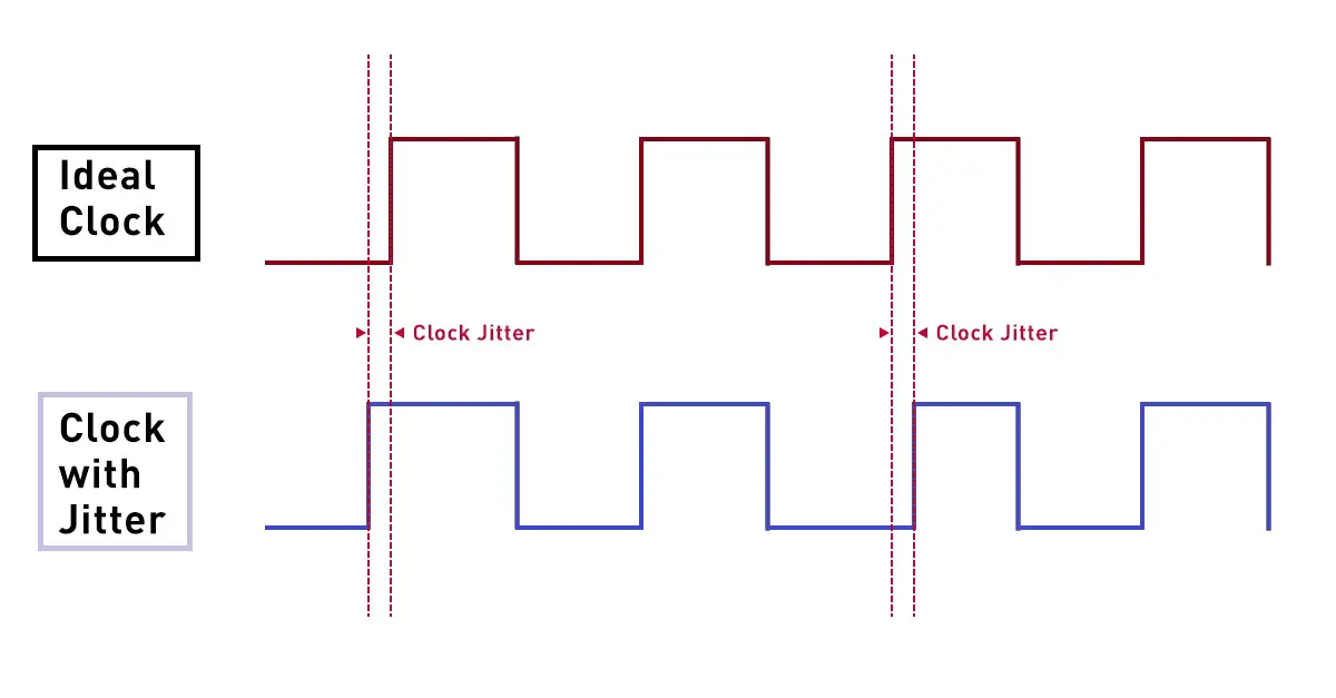
The clock signal may be made slower or faster by the jitter, thus violating the setup or hold time restrictions. The chip or circuit’s performance or functionality will suffer as a result. Therefore, it is a important factor in timing analysis and circuit design.
How many types of clock jitter are there?
Cycle to Cycle Jitter
Cycle-to-cycle jitter is the difference between two consecutive clock cycle edges within a random 1000-clock cycle. #It calculates the difference between the minimum and maximum clock edge changes.#
Phase Jitter
These are rapid and short-term fluctuations due to phase noise in the frequency domain. It can be translated into jitter values.
Phase noise = signal power/noise power, normalized at 1Hz bandwidth at a given offset from the carrier signal.#
Time interval error Jitter
It establishes the distance between each active edge and its corresponding edge on the ideal clock. The RMS TIE calculates the timing error’s standard deviation.#
Period Jitter
The variation over the RMS value of the deviation of 10,000 clock cycles is the average clock period value. Jitter during the peak-to-peak period is another name for it.#
Which type of jitters can be used to determine high-frequency jitter?
High-frequency jitter is calculated using cycle-to-cycle jitter. It represents the maximum amount of clock jitter in the random collection of clock cycles.

1 Comment
I am really loving the theme/design of your web site. Do you ever run into any browser compatibility problems? A few of my blog readers have complained about my website not working correctly in Explorer but looks great in Chrome. Do you have any tips to help fix this issue?