
What is the input resistance of a CMOS inverter?
I’ve noticed that when resistance is used instead of the PMOS transistor in a CMOS inverter circuit, it disrupts the normal operation of the circuit. In a CMOS inverter, both PMOS and NMOS transistors work together to invert the input signal, and without the PMOS, you won’t achieve the desired functionality.
The PMOS transistor’s job is to pull the output voltage to a logically high level (VDD) when the input signal is logically low (ground). It acts as a switch, allowing or blocking the current flow based on the input signal. However, if resistance is substituted for the PMOS transistor, it cannot perform its switching function properly.
Using a resistance instead of the PMOS transistor causes a continuous flow of current through the circuit. As a result, the output voltage remains constant, regardless of the input signal. The inverter loses its ability to invert the input signal and provide the expected logical levels at the output. This can significantly impact the circuit’s functionality, leading to incorrect or unpredictable operation.
Why You See High Input Resistance in a CMOS Inverter
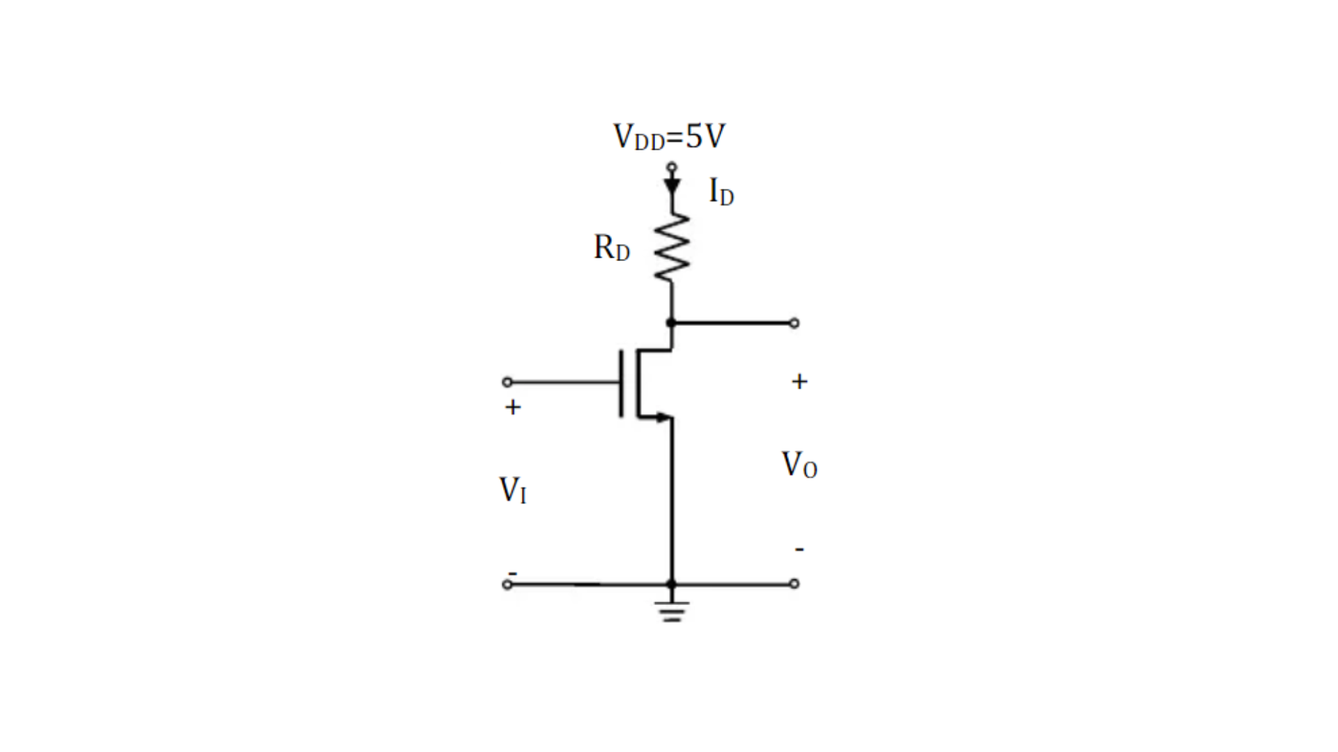
When you use a CMOS inverter, you notice its input resistance is extremely high, nearly infinite. This happens because the input connects to the gate terminals of the MOSFETs, which are separated from the drain and source by a thin oxide layer. So, the inverter takes almost no DC current from the input source.