
Equilibrium Conditions
Equilibrium or Zero Bias – No external voltage is applied to the PN junction
Under equilibrium conditions, when no external voltage is applied, a concentration gradient forms at the pn-junction. Electrons in the n-type region diffuse into the p-type region, while holes in the p-type region diffuse into the n-type region. This diffusion of charge carriers creates a negatively charged region near the pn-boundary on the p-side and a positively charged region on the n-side. This region called the depletion or space-charge region, is where the majority of carriers have been removed, leaving immobile acceptor and donor ions.
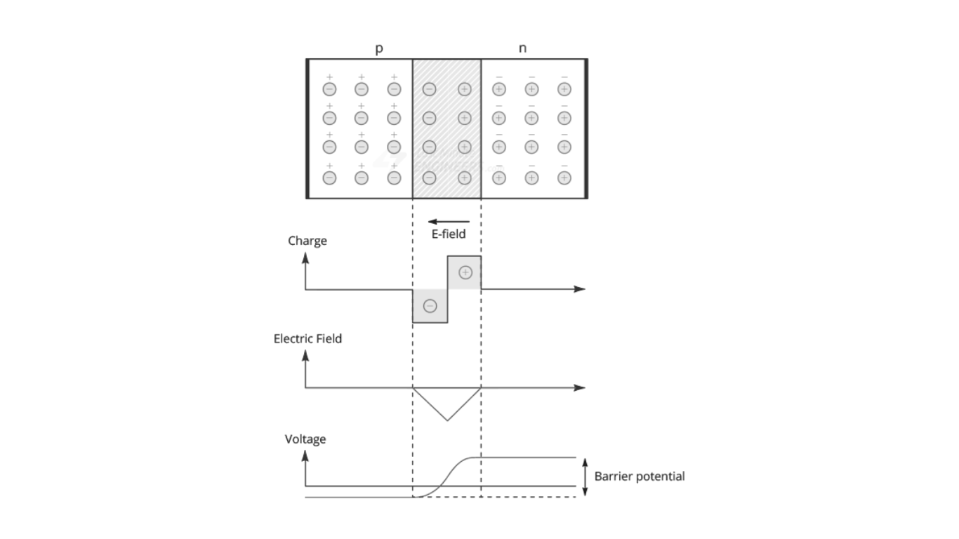
The separated charges in the depletion region create an electric field, opposing further carrier diffusion. Electrons drift from the p to the n region, and holes drift from the n to the p region due to this field. Under equilibrium, the electric field balances the diffusion, resulting in zero net current flow.
Additionally, there is a built-in potential (V0) across the junction, determined by thermal voltage (VT) and intrinsic carrier concentration (ni). This potential is a key parameter in diode behavior, and it establishes the voltage at which the diode becomes forward-biased or reverse-biased.
What happens to the behavior of a pn-junction diode when a forward voltage (VD) is applied to the junction
When a forward voltage (VD) is applied to a pn-junction diode, the potential of the p-region is raised relative to the n-region, causing a reduction in the potential barrier at the junction. This lower barrier allows mobile carriers, which are majority carriers (holes in the p-region and electrons in the n-region), to flow more freely across the junction. These carriers move through the depletion region and enter the neutral n- and p-regions, where they become minority carriers. Assuming a negligible voltage gradient across the neutral regions (typical in modern devices), these minority carriers diffuse through the region due to a concentration gradient until they recombine with majority carriers. This process results in a net current flowing through the diode, from the p-region to the n-region, and the diode is said to be in forward bias mode.
What is the basic structure of a pn-junction diode?
A pn-junction diode consists of p-type and n-type regions separated by a thin transition region, with aluminum contacts providing access to the terminals.
How are the majority carriers and doping different in the p-type and n-type materials of a diode?
In the p-type material, holes are the majority carriers, and it’s doped with acceptor impurities. In the n-type material, electrons are the majority carriers, and it’s doped with donor impurities.
What is the depletion or space-charge region in a pn-junction diode?
The depletion region is the area at the junction where the majority of carriers have been removed, leaving behind fixed acceptor and donor ions. It has a built-in electric field.
What is the significance of the built-in potential in a pn-junction diode?
The built-in potential is the voltage across the junction under zero bias. It prevents further flow of majority carriers, creating equilibrium.
What is the thermal voltage, and what is the typical value of the intrinsic carrier concentration in silicon at room temperature?
The thermal voltage is represented by fT and is related to the temperature. The intrinsic carrier concentration ni in silicon at 300 K is approximately 1.5 x 10^10 cm^-3.
What happens to the potential barrier in a pn-junction diode when a forward voltage is applied?
The applied forward voltage lowers the potential barrier, allowing mobile carriers to flow across the junction, dominated by diffusion current.
What is the consequence of applying a reverse voltage to a pn-junction diode?
Applying reverse voltage raises the potential barrier, reducing diffusion current. The drift current becomes dominant, but it’s typically very small, leading to nonconducting behavior.