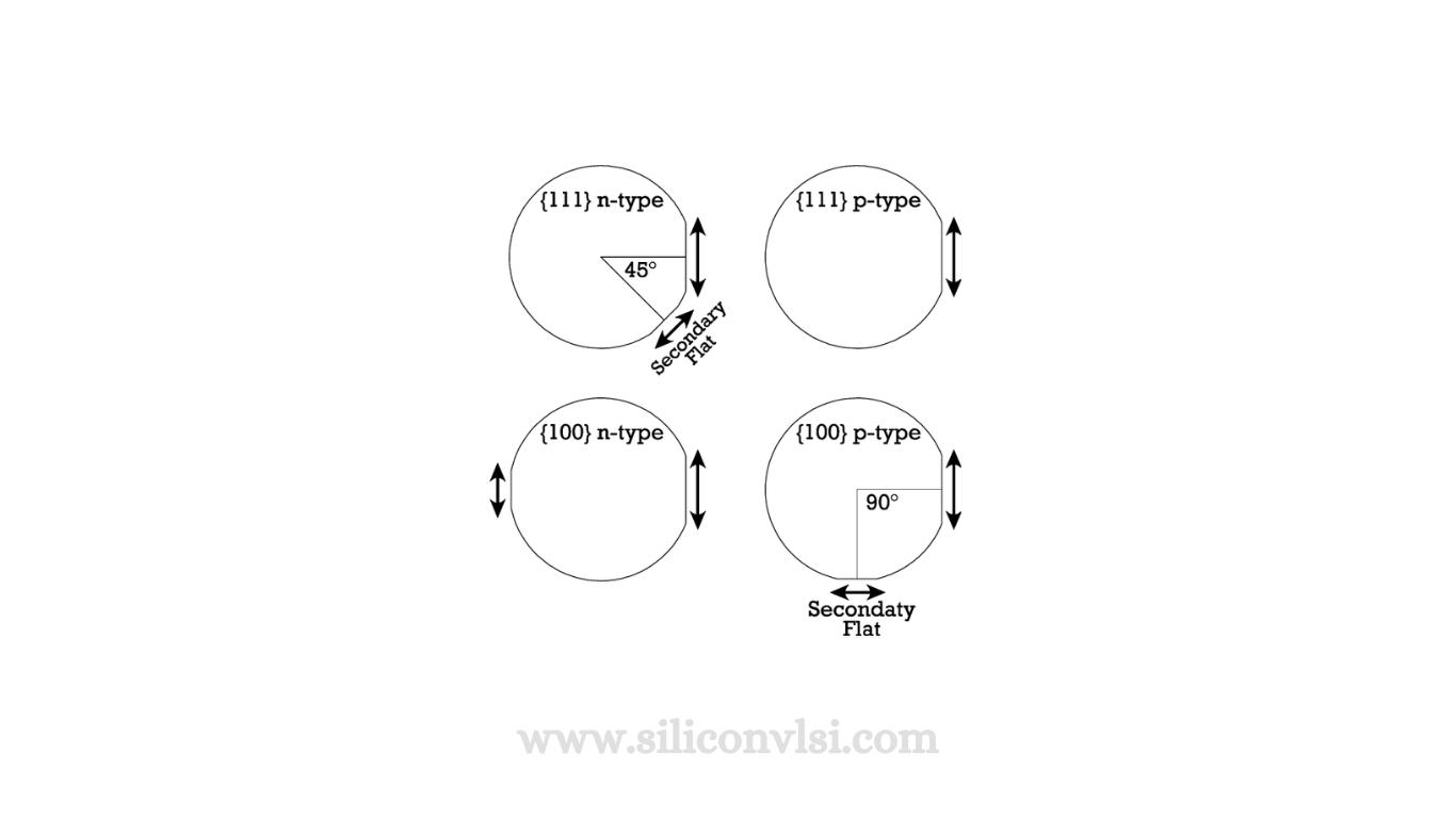
The fabrication sequence for standard bipolar integrated circuits begins with the starting material, which is a lightly doped (111)–oriented P-type substrate. The choice of (111)-oriented silicon substrates is preferred due to their ability to suppress a parasitic PMOS transistor inherent in the standard bipolar process. The wafers are typically cut off-axis to minimize pattern distortion.

In the starting material, the N-epi (N-epitaxial) layer forms the back gate of the parasitic PMOS transistor. A metal lead crossing the field oxide above the tank acts as its gate electrode. The base region within the tank serves as the source, and the drain consists of the P+ isolation. When the base diffusion is biased to a high voltage relative to the metal lead, a channel forms, allowing current to flow from the base to the isolation. This constitutes the operation of the parasitic PMOS transistor.
One distinctive aspect involves the use of (111) silicon, which artificially elevates the PMOS thick-field threshold. This is achieved by introducing positive surface-state charges along the oxide-silicon interface. The (111) silicon orientation plays a crucial role in modifying the electrical characteristics of the PMOS transistor formed under thick-field oxide, leading to an increased threshold voltage known as the thick-field threshold.