Close Menu
  • Analog Design
    • Latest Analog Layout Interview Questions (2025)
  • Digital Design
    • Digital Electronics Interview Question(2025)
    • Top VLSI Interview Questions
  • Physical Design
    • Physical Design Interview Questions for VLSI Engineers
  • Verilog
    • Verilog Interview Questions(2024)
  • Forum
Facebook Instagram YouTube LinkedIn WhatsApp
SiliconvlsiSiliconvlsi
Ask Questions Register in Forum Login in Forum
Facebook Instagram YouTube LinkedIn WhatsApp
  • Analog Design
    • Latest Analog Layout Interview Questions (2025)
  • Digital Design
    • Digital Electronics Interview Question(2025)
    • Top VLSI Interview Questions
  • Physical Design
    • Physical Design Interview Questions for VLSI Engineers
  • Verilog
    • Verilog Interview Questions(2024)
  • Forum
SiliconvlsiSiliconvlsi
Home»Digital Design»Why do we gradually increase the size of a CMOS inverter in each cascaded stage?
Digital Design

Why do we gradually increase the size of a CMOS inverter in each cascaded stage?

siliconvlsiBy siliconvlsiJune 29, 2023Updated:June 16, 2025No Comments1 Min Read
Facebook Pinterest LinkedIn Email WhatsApp
Share
Facebook Twitter LinkedIn Pinterest Email

CMOS inverter

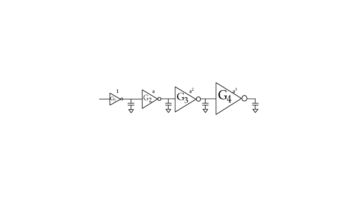
Gradually increasing the size of a CMOS inverter in each cascaded stage ensures proper signal amplification and voltage levels throughout the circuit. Increasing the size of the inverters improves the overall voltage gain, enabling larger output voltage swings and enhancing noise immunity.

This gradual size increase helps maintain signal integrity, minimize signal degradation, and boost the overall performance of the cascaded CMOS inverter circuit.

Why We Use Cascaded Buffers Instead of Just Wider Transistors

When you need to drive a heavy load quickly, a single inverter isn’t enough—so we use a buffer designed for higher speed. A CMOS gate can drive more current if we increase the transistor’s channel width. Doubling the width lets us charge a capacitor twice as fast.

But here’s the issue: doubling the channel width also doubles the gate’s input capacitance. That means the previous stage will need more time to drive it, slowing everything down. So, we must balance input capacitance and driving strength.

To solve this, we cascade multiple inverters, each with increasing channel width. The first inverter handles the input with low capacitance, and the last provides strong drive to the load.

Share. Facebook Twitter Pinterest LinkedIn Tumblr Email

Related Posts

Difference Between Clipper and Clamper

June 22, 2025

Understanding the Difference Between RAM Bandwidth and Clock Speed

December 1, 2024

Why is Frequency Planning so important in Module Design?

September 2, 2024
Leave A Reply Cancel Reply

Facebook X (Twitter) Instagram Pinterest Vimeo YouTube
  • About Us
  • Contact Us
  • Privacy Policy
© 2025 Siliconvlsi.

Type above and press Enter to search. Press Esc to cancel.