
3-to-8 Decoder Verilog Code
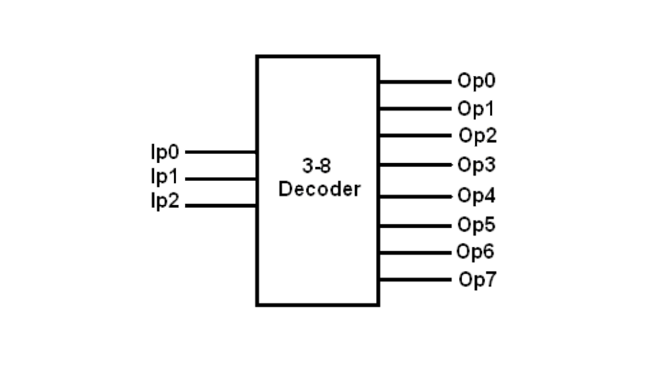
A 3-to-8 decoder is a combinational logic device that takes three input lines and produces eight output lines. For each possible combination of the three input binary lines, one and only one output signal will be logic 1. The decoder acts as a min-term generator, where each output corresponds to one min-term. Decoders find various applications in the design of digital systems.
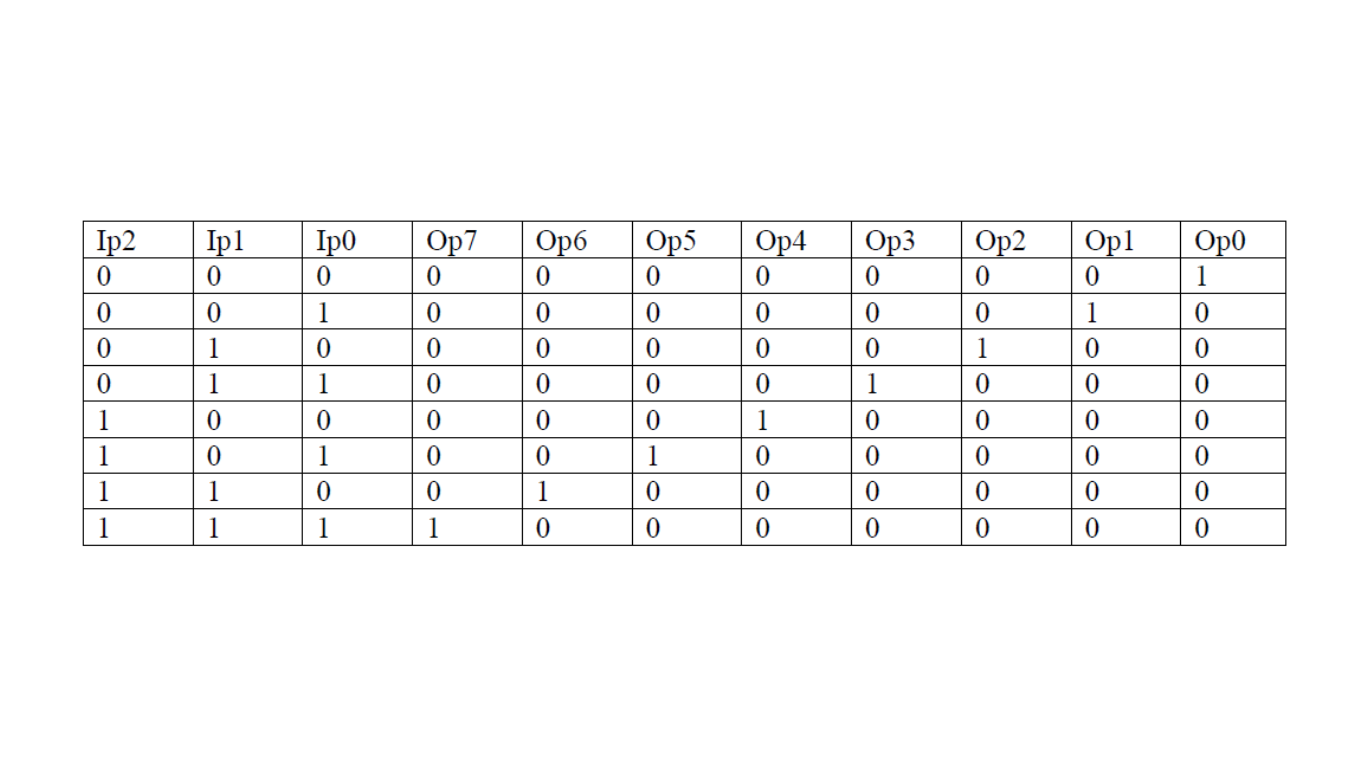
Truth Table for 3-to-8 Decoder
The truth table for the 3-to-8 decoder is shown in Figure 2. The inputs Ip0 to Ip2 are the binary input lines, and the outputs Op0 to Op7 represent the eight output lines.
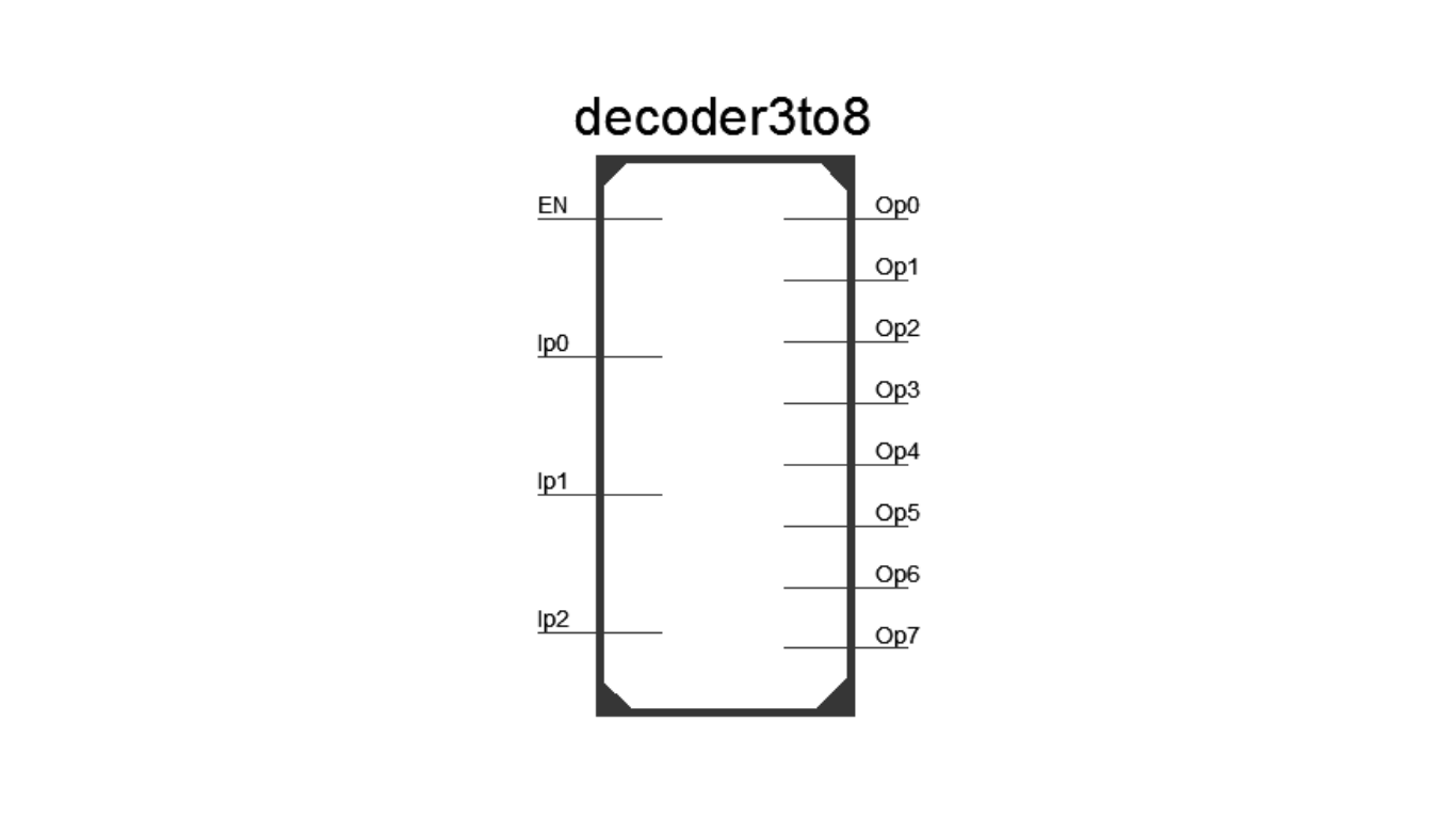
Verilog Module: 3-to-8 Decoder
Figure 3 displays the Verilog module of the 3-to-8 decoder. The module takes three 1-bit binary values from the input ports Ip0 to Ip2. The eight 1-bit binary outputs are presented in eight output ports Op0 to Op7. The decoder function is controlled by the enable signal, EN.
Verilog Code for 3-to-8 Decoder
module decoder3to8(
input Ip0,
input Ip1,
input Ip2,
input EN,
output reg Op0=0,
output reg Op1=0,
output reg Op2=0,
output reg Op3=0,
output reg Op4=0,
output reg Op5=0,
output reg Op6=0,
output reg Op7=0
);
always @ (EN, Ip2, Ip1, Ip0)
begin
Op0 = 0;
Op1 = 0;
Op2 = 0;
Op3 = 0;
Op4 = 0;
Op5 = 0;
Op6 = 0;
Op7 = 0;
if (EN == 1’b1)
begin
case ({Ip2, Ip1, Ip0})
3’b000: Op0 = 1;
3’b001: Op1 = 1;
3’b010: Op2 = 1;
3’b011: Op3 = 1;
3’b100: Op4 = 1;
3’b101: Op5 = 1;
3’b110: Op6 = 1;
3’b111: Op7 = 1;
default: begin
Op0 = 0;
Op1 = 0;
Op2 = 0;
Op3 = 0;
Op4 = 0;
Op5 = 0;
Op6 = 0;
Op7 = 0;
end
encase
end
end
endmodule
Verilog Test Bench: 3-to-8 Decoder
The Verilog test bench for the 3-to-8 decoder is demonstrated in Figure 5. It tests the functionality of the decoder by providing stimulus to the input ports (Ip0 to Ip2) and observing the output ports (Op0 to Op7) based on different values of the enable signal (EN).
module decoder3to8_tb;
// Inputs
reg Ip0;
reg Ip1;
reg Ip2;
reg EN;
// Outputs
wire Op0;
wire Op1;
wire Op2;
wire Op3;
wire Op4;
wire Op5;
wire Op6;
wire Op7;
//temporary variable
reg [2:0] count = 3’d0;
// Instantiate the Unit Under Test (UUT)
decoder3to8 uut (
.Ip0(Ip0),
.Ip1(Ip1),
.Ip2(Ip2),
.Op0(Op0),
.Op1(Op1),
.Op2(Op2),
.Op3(Op3),
.Op4(Op4),
.Op5(Op5),
.Op6(Op6),
.Op7(Op7),
.EN(EN)
);
initial begin
// Initialize Inputs
Ip0 = 1’b0;
Ip1 = 1’b0;
Ip2 = 1’b0;
EN = 1’b0;
// Wait 100 ns for global reset to finish
#100;
// Add stimulus here
EN = 1’b1;
#20;
for (count = 0; count < 8; count = count + 1’b1) begin
{Ip0, Ip1, Ip2} = {Ip0, Ip1, Ip2} + 1’b1;
#20;
end
EN = 1’b0;
end
endmodule
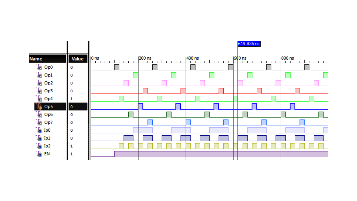
Timing Diagram for 3-to-8 Decoder
The following figure presents the timing diagram of the 3-to-8 decoder, illustrating the waveforms of the output ports (Op0 to Op7) as the input lines are selected based on different values of the enable signal (EN).
The 3-to-8 decoder is a fundamental building block in digital systems that enables selecting one of the eight outputs based on the binary input lines. The provided Verilog module and test bench ensure the correct functionality of the decoder for different input selections.