
Verilog Code for 4-bit Carry Ripple Adder
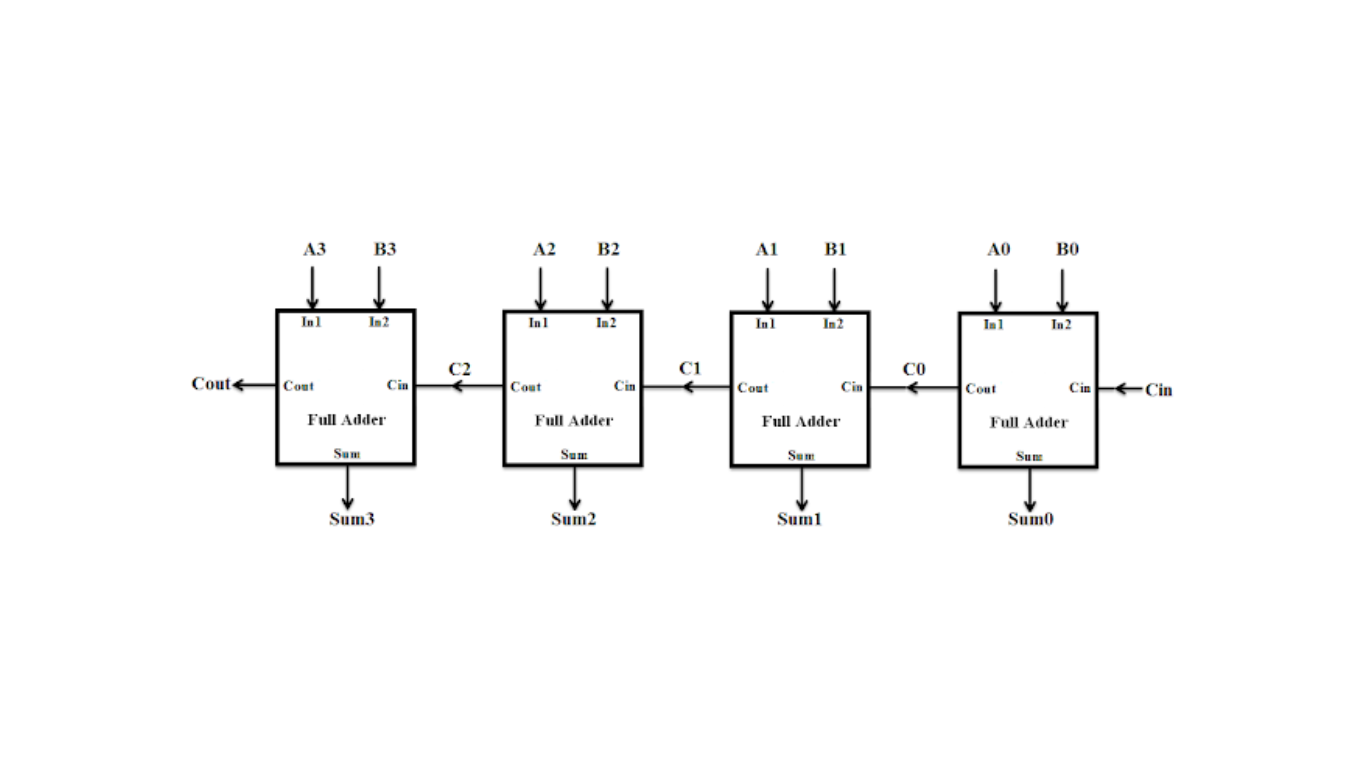
A 4-bit carry ripple adder is a circuit that adds two 4-bit binary numbers using four cascaded 1-bit full adders. Each full adder takes a carry-in (Cin), which is the carry-out (Cout) of the previous adder, forming a ripple-carry adder. In this design, each carry-bit “ripples” to the next full adder, enabling the addition of multi-bit numbers. The simplicity of the layout allows for fast design time, but the adder’s performance is relatively slower due to the ripple propagation delay. Figure 1 illustrates a 4-bit carry ripple adder formed by cascading four full adders.
Verilog Module: 4-bit Carry Ripple Adder
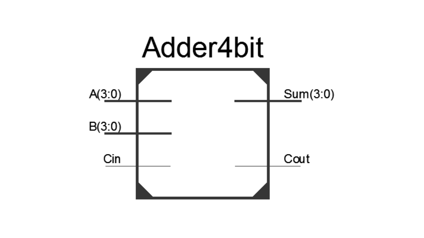
Figure 2 presents the Verilog module for the 4-bit carry ripple adder. It contains two 4-bit input ports (A and B) used to read the two 4-bit numbers to be added. The 1-bit carry-in input port (Cin) is used to read a carry bit if another instance of the ripple carry adder is cascaded to a less significant stage. The 4-bit sum generated by the adder is presented in the 4-bit output port (Sum), and the 1-bit carry-out is available in the Cout output port. The carry-out, Cout, provides a carry-bit if another instance of the ripple carry adder is cascaded to a more significant stage.
Truth table for a 4-bit carry ripple adder
| A (4-bit) | B (4-bit) | Cin | Sum (4-bit) | Cout |
|---|---|---|---|---|
| 0000 | 0000 | 0 | 0000 | 0 |
| 0000 | 0000 | 1 | 0001 | 0 |
| 0000 | 0001 | 0 | 0001 | 0 |
| 0000 | 0001 | 1 | 0010 | 0 |
| 0000 | 0010 | 0 | 0010 | 0 |
| 0000 | 0010 | 1 | 0011 | 0 |
| … | … | … | … | … |
| 1111 | 1110 | 1 | 11001 | 1 |
| 1111 | 1111 | 0 | 1110 | 1 |
| 1111 | 1111 | 1 | 1111 | 1 |
In the truth table, A and B represent the two 4-bit binary numbers being added, and Cin is the carry-in bit. The output Sum is the result of the addition, represented as a 4-bit binary number. The output Cout is the carry-out bit, which will be propagated to a more significant stage if the adder is part of a larger multi-bit adder. The table shows all possible combinations of inputs and their corresponding outputs for a 4-bit carry ripple adder.
Verilog Code for 4-bit Carry Ripple Adder
module Adder4bit(
input [3:0] A,
input [3:0] B,
input Cin,
output [3:0] Sum,
output Cout
);
wire [2:0] transferC;
fullAdder FA1 ( .In1(A[0]),
.In2(B[0]),
.Cin(Cin),
.Sum(Sum[0]),
.Cout(transferC[0])
);
fullAdder FA2 ( .In1(A[1]),
.In2(B[1]),
.Cin(transferC[0]),
.Sum(Sum[1]),
.Cout(transferC[1])
);
fullAdder FA3 ( .In1(A[2]),
.In2(B[2]),
.Cin(transferC[1]),
.Sum(Sum[2]),
.Cout(transferC[2])
);
fullAdder FA4 ( .In1(A[3]),
.In2(B[3]),
.Cin(transferC[2]),
.Sum(Sum[3]),
.Cout(Cout)
);
endmodule
Verilog Test Bench: 4-bit Carry Ripple Adder
The Verilog test bench for the 4-bit carry ripple adder is demonstrated in Figure 4. It tests the functionality of the adder by providing stimulus to the input ports (A, B, and Cin) and observing the output ports (Sum and Cout).
module Adder4bit_tb;
// Inputs
reg [3:0] A;
reg [3:0] B;
reg Cin;
// Outputs
wire [3:0] Sum;
wire Cout;
// Instantiate the Unit Under Test (UUT)
Adder4bit uut (
.A(A),
.B(B),
.Cin(Cin),
.Sum(Sum),
.Cout(Cout)
);
initial begin
// Initialize Inputs
A = 4’b0;
B = 4’b0;
Cin = 4’b0;
// Wait 100 ns for global reset to finish
#100;
// Add stimulus here
A = 4’b1011;
B = 4’b0100;
Cin = 4’b0;
#20;
A = 4’d1111;
B = 4’d1101;
Cin = 4’b1;
end
endmodule
Timing Diagram
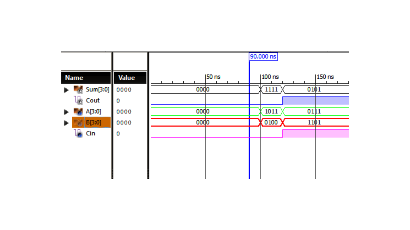
Figure 3 displays the timing diagram of the 4-bit carry ripple adder, illustrating the propagation of carry and sum values as the input numbers are added.
The 4-bit carry ripple adder is a fundamental building block for arithmetic operations in digital systems. It is suitable for adding 4-bit numbers but can be extended to larger bit widths by cascading additional stages of full adders. The provided Verilog module and test bench enable efficient and accurate addition of binary numbers using this cascade approach.