
A full adder is a important component in digital circuit design, capable of adding two 1-bit binary numbers along with a 1-bit carry-in to produce a 1-bit sum and a 1-bit carry-out. The input signals A and B represent the two 1-bit values to be added, and Cin is the carry-in from the preceding significant bit of the calculation. The sum (S) and carry-out (Cout) can be determined using the following Boolean expressions:
- S = A xor B xor Cin
- Cout = (A and B) or (B and Cin) or (Cin and A)
Full adders are often cascaded together to add larger binary numbers, such as 4, 8, 16, or 32 bits.
Gate-Level Design of a Full Adder
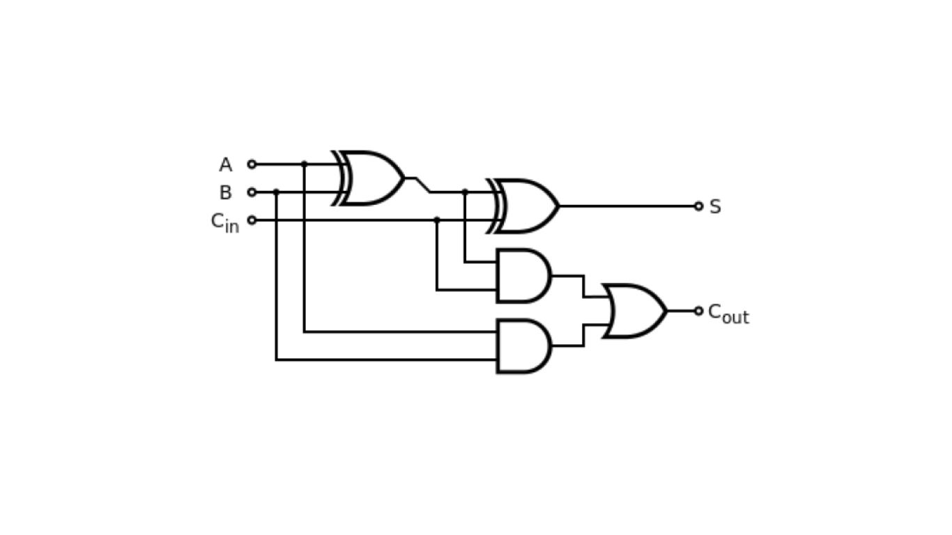
The gate-level design of a full adder is represented as shown in Figure 1. It employs logic gates to compute the sum and carry-out based on the input signals A, B, and Cin.
Truth Table for Full Adder
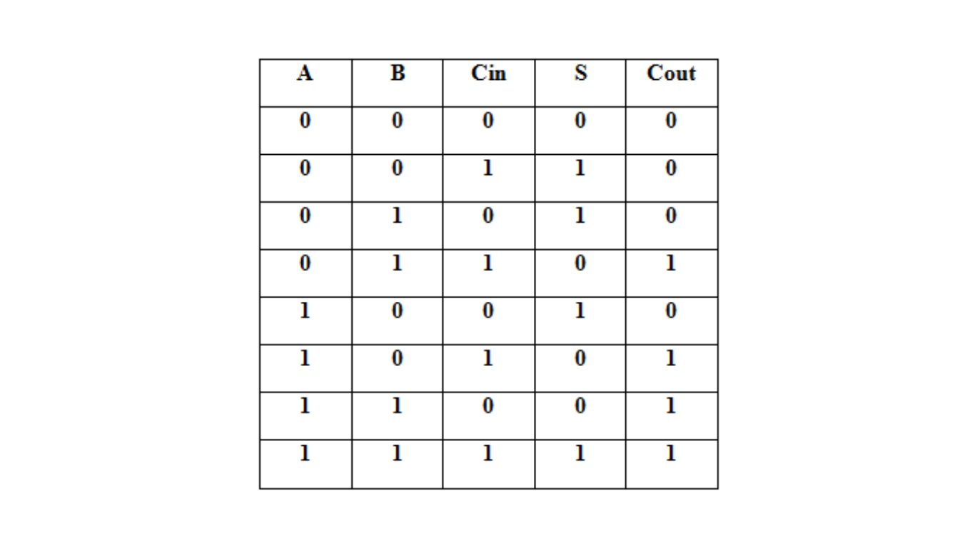
The truth table for a typical full adder is shown in Figure 2. It shows all possible combinations of the three input signals (A, B, and Cin) and their corresponding sum (S) and carry-out (Cout) outputs.
Verilog Module for Full Adder
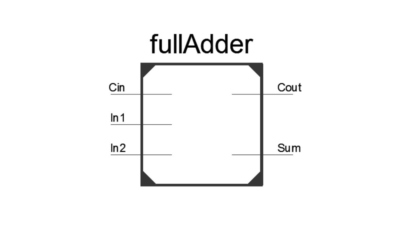
The Verilog module implementation of a full adder is depicted in Figure 3. It includes three 1-bit input ports (In1, In2, and Cin) and two 1-bit output ports (Sum and Cout).
Verilog Code of the Full Adder
module fullAdder (
input In1,
input In2,
input Cin,
output Sum,
output Cout
);

assign Sum = (In1 ^ In2) ^ Cin;
assign Cout = (In1 & In2) | (In2 & Cin) | (Cin & In1);

endmodule
Verilog Test Bench for Full Adder
To verify the functionality of the full adder, a Verilog test bench is used. The code for the test bench is shown in Figure
`timescale 1ns / 1ps
module fullAdder_tb;
// Inputs
reg In1;
reg In2;
reg Cin;
// Outputs
wire Sum;
wire Cout;
// Temporary looping variable
reg [2:0] i = 3’d0;
// Instantiate the Unit Under Test (UUT)
fullAdder uut (
.In1(In1),
.In2(In2),
.Cin(Cin),
.Sum(Sum),
.Cout(Cout)
);
initial begin
// Initialize Inputs
In1 = 1’b0;
In2 = 1’b0;
Cin = 1’b0;
// Wait 100 ns for global reset to finish
#100;
// Add stimulus here
for (i = 0; i < 8; i = i + 1’b1) begin
{In1, In2, Cin} = {In1, In2, Cin} + 1’b1;
#20;
end
end
end module
With this understanding of the full adder, you can utilize its capability to perform binary addition with carry. By implementing the Verilog module and test bench, you can seamlessly integrate the full adder into more extensive digital systems to perform complex arithmetic operations.