
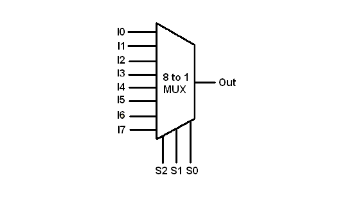
8-to-1 Multiplexer: Selecting Among Eight Inputs
An 8-to-1 multiplexer is a digital device that allows the selection of one of the eight input lines to be transmitted to the output line based on a three-bit selection line. The block diagram of the 8-to-1 multiplexer is shown in Figure 1. For a 2n-to-1 multiplexer, it requires n bits of selection lines to choose one out of the 2n inputs for the output.
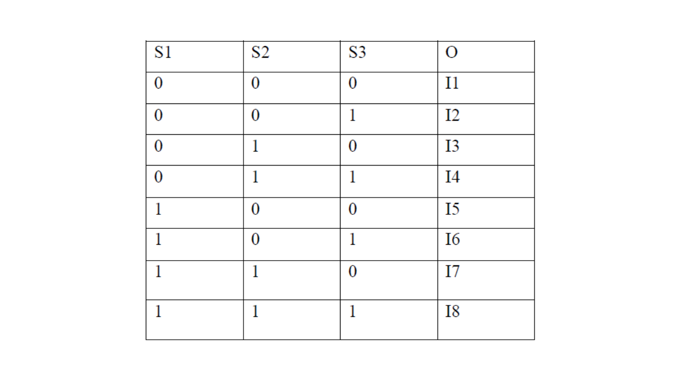
Truth Table for 8-to-1 Multiplexer
The truth table for the 8-to-1 multiplexer is shown in Figure 2. In this table, I1 to I8 represent the input lines, S1 – S3 are the selection lines, and O is the output line.
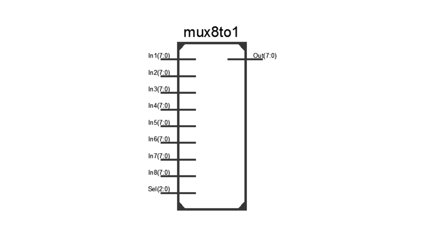
Verilog Module: 8-to-1 Multiplexer
Figure 3 displays the Verilog module for the 8-to-1 multiplexer. The module includes eight 8-bit input ports (In1 to In8) representing the input lines of the multiplexer. The three-bit port Sel is the selection line used to select one of the eight input lines and the 8-bit port Out represents the output line of the multiplexer.
Verilog Code for the 8-to-1 Multiplexer
module mux8to1(
output reg [7:0] Out,
input [2:0] Sel,
input [7:0] In1,
input [7:0] In2,
input [7:0] In3,
input [7:0] In4,
input [7:0] In5,
input [7:0] In6,
input [7:0] In7,
input [7:0] In8
);
always @ (In1 or In2 or In3 or In4 or In5 or In6 or In7 or In8 or Sel)
begin
case (Sel)
3’b000 : Out = In1;
3’b001 : Out = In2;
3’b010 : Out = In3;
3’b011 : Out = In4;
3’b100 : Out = In5;
3’b101 : Out = In6;
3’b110 : Out = In7;
3’b111 : Out = In8;
default : Out = 8’bx; // If input is undefined, then output is undefined
endcase
end
endmodule
The Verilog test bench for the 8-to-1 multiplexer is demonstrated in Figure 5. It tests the functionality of the multiplexer by providing stimulus to the input ports (In1 to In8) and observing the output port Out based on different selections (Sel).
module mux8to1_tb;
// Inputs
reg [2:0] Sel;
reg [7:0] In1;
reg [7:0] In2;
reg [7:0] In3;
reg [7:0] In4;
reg [7:0] In5;
reg [7:0] In6;
reg [7:0] In7;
reg [7:0] In8;
// Outputs
wire [7:0] Out;
// Instantiate the Unit Under Test (UUT)
mux8to1 uut (
.Out(Out),
.Sel(Sel),
.In1(In1),
.In2(In2),
.In3(In3),
.In4(In4),
.In5(In5),
.In6(In6),
.In7(In7),
.In8(In8)
);
initial begin
// Initialize Inputs
Sel = 0;
In1 = 0;
In2 = 0;
In3 = 0;
In4 = 0;
In5 = 0;
In6 = 0;
In7 = 0;
In8 = 0;
// Wait 100 ns for global reset to finish
#100;
// Add stimulus here
Sel = 3’d0;
In1 = 8’d0;
In2 = 8’d1;
In3 = 8’d2;
In4 = 8’d3;
In5 = 8’d4;
In6 = 8’d5;
In7 = 8’d6;
In8 = 8’d7;
// Selection input generation
for (count = 0; count < 8; count = count + 1’b1) begin
Sel = count;
#20;
end
end
endmodule
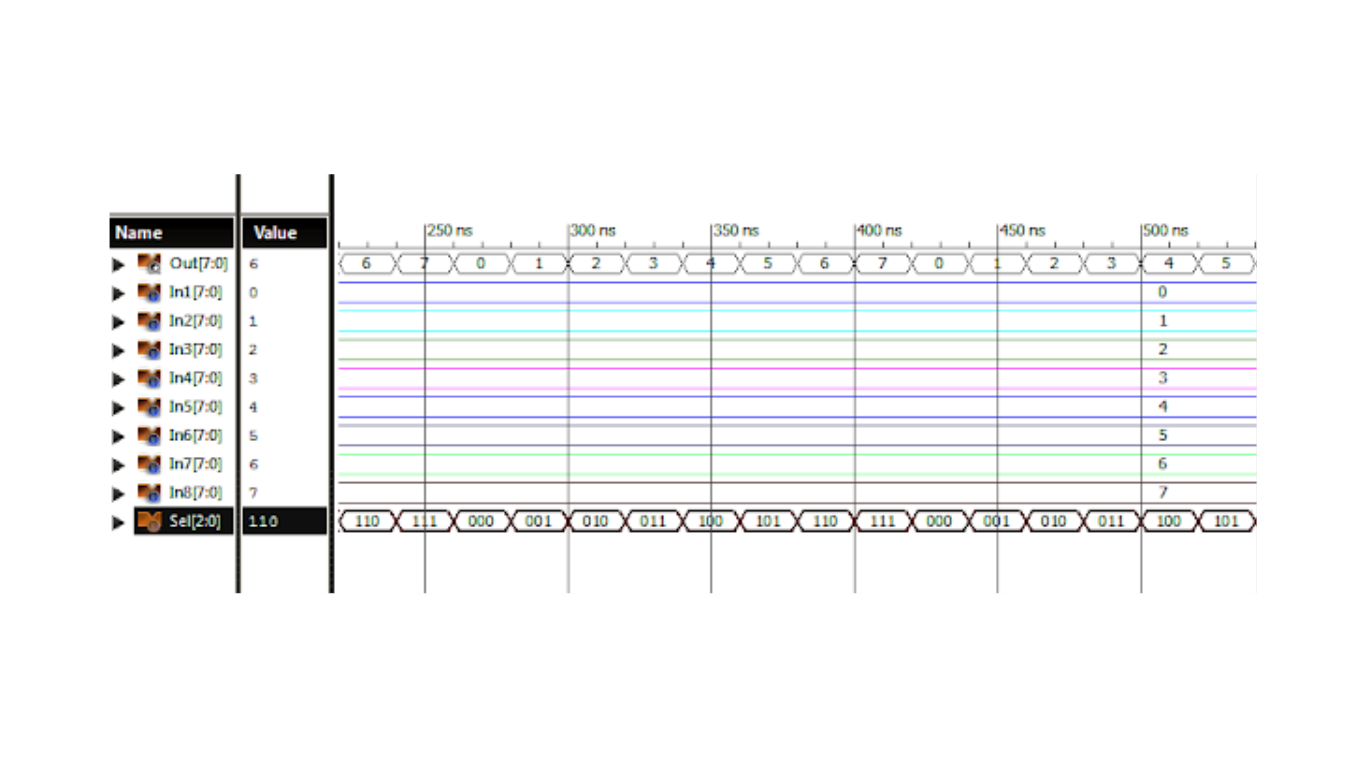
Timing Diagram for 8-to-1 Multiplexer
The following figure presents the timing diagram of the 8-to-1 multiplexer, illustrating the waveforms of the output Out as the input lines are selected based on different values of the selection lines Sel.
The 8-to-1 multiplexer is an essential building block in digital systems that enables selecting one of multiple input lines based on the control signals. The provided Verilog module and test bench ensure the correct functionality of the multiplexer for different input selections.