Analog and Memory Layout Design Forum
To find the answer to any of the following questions, simply copy the question and paste it into the search box. You’ll get the exact answer you’re looking for. Give it a try now!
Are there alternative deposition techniques for metallic interconnect materials like copper?
At room temperature, what type of temperature coefficient is typically observed in resistors, and why?
Can you describe the starting point of the FEOL process and the initial steps involved?
Can you explain the basic process steps involved in the low-k/Cu dual damascene backend?
Can you explain the steps involved in folding a FET with an example?
Differences between Wet etching and Dry (plasma) Etching
Does NWELL have any impact on NMOS, do we have to consider WPE for NMOS
How are lightly doped p- and n-wells formed in the CMOS fabrication process?
How are static memories designed to preserve data?
How are the functionalities of a CMOS circuit determined in terms of layers?
How are the gate sidewall spacers formed in the source/drain module, and what functions do they serve in the semiconductor fabrication process?
How are the majority carriers and doping different in the p-type and n-type materials of a diode?
How are the threshold voltages of PMOS and NMOS transistors adjusted in CMOS fabrication?
How are variations in the width (W) and length (L) of transistors typically caused in integrated circuits?
How can floorplanning impact the performance of a mixed-signal circuit?
How can latch-up be prevented in CMOS processes, and what role do resistances Rnwell and Rpsubs play in this prevention?
How can noise signals enter a digital circuit?
How can the discrete movement of charge related to shot noise affect the behavior of electronic components like diodes or MOSFETs?
How can the interwire capacitance between signals on different layers be reduced further?
How can the skin effect impact the performance of digital circuits?
How can you address the issue of voltage fluctuations caused by occasional high current demands in CMOS circuits?
How can you mitigate ground bounce issues in a circuit?
How can you reduce the sensitivity to cross-talk in nodes, such as precharged buses?
How do dynamic memories work, and what is the key principle behind their operation?
How do short-channel and narrow-channel effects impact the threshold voltage?
How do short-channel and narrow-channel effects interact, and what happens when both are present in small geometry transistors?
How do state-of-the-art MOSFET technologies address the hot-carrier effect to ensure long-term reliability?
How do variations in wire width and line spacing impact interconnect performance?
How does CMP work?
How does diffusion implantation work, and what conditions are typically required for this process?
How does dynamic storage in sequential circuits differ from static storage?
How does gate array customization take place?
How does increasing VDS affect the effective channel length in a MOS transistor?
How does increasing VDS affect the effective channel length in a MOS transistor, and what impact does this have on the drain current?
How does Nyquist’s theory relate to the prevention of aliasing errors in signal processing?
How does plasma etching work, and what are its advantages in semiconductor manufacturing?
How does temperature affect the diode current, and what are the two temperature-dependent factors mentioned?
How does the addition of a bleeder transistor help counteract charge leakage in dynamic circuits?
How does the application of a positive voltage to the gate affect the semiconductor material beneath it?
How does the bistable circuit store information?
How does the choice of interlayer dielectric (ILD) material impact interconnect capacitance and the associated RC delay?
How does the choice of substrate and the well process impact the quality and performance of PMOS devices?
How does the CMFB amplifier achieve its goal of regulating the common-mode voltage in the differential amplifier outputs?
How does the critical field for electron saturation in p-type silicon compare to that for hole saturation?
How does the critical field for electron saturation in p-type silicon compare to that for hole saturation?
How does the density of a full-custom layout compare to that of a standard-cell layout, both using the same process?
How does the depletion region beneath the gate affect the threshold voltage, especially in short-channel devices?
How does the drain current behave in the saturation region of a MOSFET?
How does the dual damascene process address the challenges associated with limited depth-of-focus optics in via patterning?
How does the exposure and development process affect the photoresist during PCB fabrication?
How does the gate voltage affect the conductivity of the channel in a MOSFET?
How does the gate voltage affect the conductivity of the channel in a MOSFET?
How does the hot-carrier effect contribute to the long-term reliability challenges in integrated circuits?
How does the hot-carrier effect contribute to the long-term reliability challenges in integrated circuits?
How does the impedance of Vin affect the injected charge in MOSFET switching?
How does the impedance of Vin affect the injected charge in MOSFET switching?
How does the inter-wire capacitance impact integrated circuits in multi-layer interconnect structures?
How does the inter-wire capacitance impact integrated circuits in multi-layer interconnect structures?
How does the presence of the polysilicon gate contribute to the self-alignment of the source/drain extensions in the semiconductor manufacturing process?
How does the presence of the polysilicon gate contribute to the self-alignment of the source/drain extensions in the semiconductor manufacturing process?
How does the relationship between carrier mobility and carrier concentration influence the temperature coefficient of a resistor?
How does the relationship between carrier mobility and carrier concentration influence the temperature coefficient of a resistor?
How does the sizing of the load device in pseudo-NMOS logic impact its performance characteristics?
How does the sizing of the load device in pseudo-NMOS logic impact its performance characteristics?
How does the transition from the on- to off-condition in a MOS transistor with decreasing gate-source voltage differ from an ideal switch-like behavior?
How does the transition from the on- to off-condition in a MOS transistor with decreasing gate-source voltage differ from an ideal switch-like behavior?
How does the use of guard rings enhance the performance of mixed-signal circuits?
How does the use of guard rings enhance the performance of mixed-signal circuits?
How is a folded FET constructed in terms of subtransistors?
How is a folded FET constructed in terms of subtransistors?
How is chemical-mechanical polishing (CMP) used in semiconductor manufacturing, and what challenges does it pose for achieving planarity?
How is chemical-mechanical polishing (CMP) used in semiconductor manufacturing, and what challenges does it pose for achieving planarity?
How is polysilicon deposited on a wafer, and what is the purpose of this material in semiconductor manufacturing?
How is positive feedback achieved in a CMOS Schmitt trigger circuit?
How is positive feedback achieved in a CMOS Schmitt trigger circuit?
How is standard cell design supported in terms of libraries and EDA tools?
How is standard cell design supported in terms of libraries and EDA tools?
How is the base width of the NPN transistor defined?
How is the base width of the NPN transistor defined?
How is the complexity of an IC measured?
How is the complexity of an IC measured?
How is the conductivity of semiconductors different from metals and insulators?
How is the conductivity of semiconductors different from metals and insulators?
How is the continuous range of values of an electrical node voltage transformed into a discrete variable in digital circuit representation?
How is the continuous range of values of an electrical node voltage transformed into a discrete variable in digital circuit representation?
How is the design implementation process different between FPGA chips and GA chips?
How is the design implementation process different between FPGA chips and GA chips?
How is the resistance of a wire related to its length and cross-sectional area?
How is the saturation region of a MOSFET defined?
How is the saturation region of a MOSFET defined?
How is the sizing of an NPN transistor achieved?
How is the static power dissipation associated with a bleeder transistor eliminated in dynamic circuits?
How is the threshold voltage (VT) defined for a MOSFET, and what factors influence its value?
How many terminals does a MOSFET (Metal-Oxide-Semiconductor Field-Effect Transistor) have, and what is the primary function of the fourth terminal?
How to do Fan-out and Fan-in Impact the Circuit Performance
In a complementary MOS technology (CMOS), what types of MOSFET devices are used, and how are they typically represented in circuit symbols?
In modern CMOS processes, why is the semiconductor surface often not flat?
In semiconductor manufacturing, what is the purpose of depositing layers of material on a wafer?
In what scenarios are dynamic memories particularly beneficial?
In which types of electronic devices is shot noise typically not present, and under what conditions does it become significant?
Use of Polysilicon Gate
Voltage Transfer Characteristic (VTC)
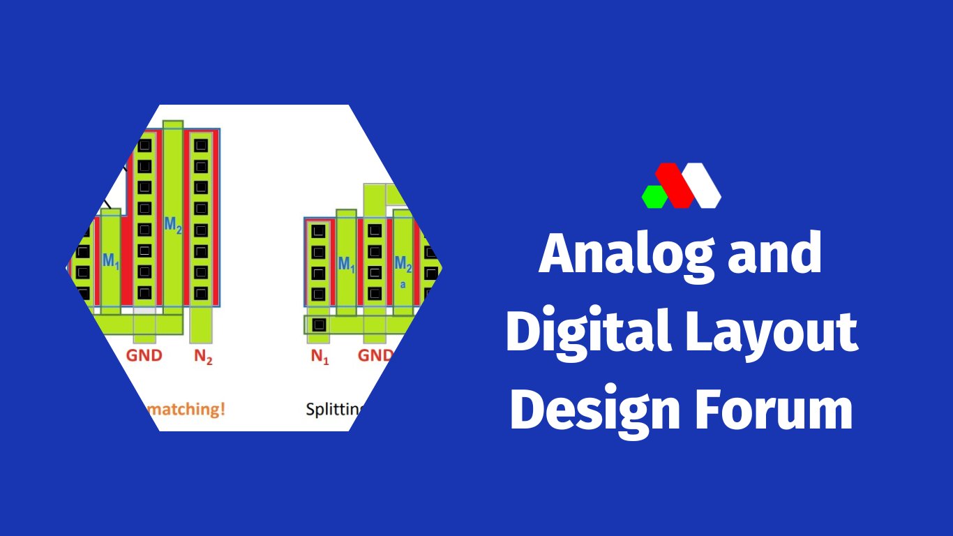
What additional layout strategies can improve analog circuit performance?
What advantage does Copper have over Aluminum as an interconnect material?
What advantages does oxide isolation offer over junction isolation in terms of transistor performance?
What are “channels” in gate array platforms, and how are they used?
What are Electromigration (EM) and IR-Drop and its prevention?
What are noise margins, and why are they important in the context of digital circuits?
What are noise margins, and why are they important in the context of digital circuits?
What are scalable design rules?
What are silicides, and why are they used in integrated circuits?
What are some advantages of folding transistors in integrated circuit design?
What are some disadvantages associated with using FPGAs compared to real ASICs (Application-Specific Integrated Circuits)?
What are some examples of standard ICs, and how do they differ from ASICs?
What are some key design goals for ASICs?
What are systematic errors in clock distribution, and how can they be addressed in chip design?
What are the adverse effects of counter-doping the p-substrate to create an n-well, and why is it not as favorable as using intrinsic silicon?
What are the adverse effects of counter-doping the p-substrate to create an n-well, and why is it not as favorable as using intrinsic silicon?
What are the benefits of CMP in semiconductor manufacturing?
What are the key advantages of using a dummy switch in charge injection management compared to other methods?
What are the key components that make up a module’s high-level behavior in functional design?
What are the key steps involved in the Functional and Logic design of Integrated Circuits?
What are the main causes of skew in clock distribution within an integrated circuit?
What are the Main Differences between wet and dry oxide growth in CMOS?
What are the main disadvantages of junction-isolated transistors?
What are the major challenges associated with clock distribution in digital circuits?
What are the practical implications of temperature dependence on diode current for digital circuits?
What are the primary entities that make up a CMOS design from a designer’s perspective?
What are the primary factors contributing to variations in transistor parameters in integrated circuits?
What are the primary objectives of circuit designers and process engineers in semiconductor manufacturing?
What are the three major factors contributing to load capacitance (CL) in a gate?
What are the two common technologies for crystal growth in silicon manufacturing?
What are the two main methods used for introducing dopants into semiconductor materials during integrated circuit manufacturing?
What are the two main solutions to prevent aliasing errors in data acquisition systems?
What are the two main types of MOSFET devices?
What are the two types of impurity atoms used in doping semiconductors?
What are VIH and VIL, and why are they significant in digital circuits?
What challenges are associated with the stability of the CMFB loop, and how can stability be achieved in practice?
What challenges arise when analog and digital circuits share the same power supply and ground connections?
What challenges does Drain-Induced Barrier Lowering (DIBL) pose in dynamic memories?
What condition leads to the pinching off of the conducting channel in a MOSFET?
What conditions are necessary for an electron to become “hot” and contribute to the hot-carrier effect?
What deposition process is typically used for aluminum interconnect layers in semiconductor manufacturing, and how is it carried out?
What determines whether a MOSFET acts as a switch and allows current to flow between the source and drain terminals?
What distinguishes a positive latch from a negative latch?
What distinguishes the contextual aspect ratio of cells in a full-custom layout from the fixed aspect ratio of standard cells?
What does the transient behavior of a CMOS inverter gate primarily depend on?
What economic dilemma do circuit designers face when dealing with variations in integrated circuit parameters?
What factors influence the choice of design style in ASIC design?
What happens to the charge under the gate oxide when the MOSFET switch turns off?
What happens to the potential barrier in a pn-junction diode when a forward voltage is applied?
What happens to the resistance between the drain and source terminals of a MOSFET when the gate-source voltage (VGS) is set to 0 and all terminals are grounded?
What happens to the resistance of a semiconductor wire when the skin effect is in play?
What happens to the reverse current of a diode when the reverse bias exceeds a certain level known as the breakdown voltage?
What happens to the thickness of the conducting channel in a MOSFET as the drain-source voltage increases?
What is a major disadvantage of pseudo-NMOS logic, particularly when the output is low?
What is a potential disadvantage of standard cell design?
What is a significant drawback of ion implantation, and how is it typically addressed?
What is Annealing?
What is avalanche breakdown in diodes, and under what conditions does it occur?
What is contact resistance, and why is it important in integrated circuit design?
What is Drain-Induced Barrier Lowering (DIBL), and how does it impact the threshold voltage?
What is dry or plasma etching, and how does it differ from wet etching?
What is hysteresis in the context of a Schmitt trigger?
What is ion implantation, and how does it differ from diffusion implantation in terms of dopant introduction?
What is Punch-Through, and why is it a concern in MOS transistors?
What is sheet resistance, and how is it related to the resistance of a square conductor?
What is subthreshold or weak-inversion conduction in a MOS transistor?
What is the “secret” behind the Schmitt trigger concept?
What is the difference between a positive resist process and a negative resist process?
What is the difference between n-doped and p-doped semiconductors?
What is the disadvantage of using Copper in interconnects?
What is the Dual Damascene process?
What is the final step in the CMOS fabrication process after depositing the metallic interconnect layers and passivation layer?
What is the fringing capacitance, and why is it important in wire capacitance modeling?
What is the function of the bleeder resistance in dynamic circuits?
What is the function of the mask in PCB fabrication?
What is the function of the sacrificial silicon nitride layer in CMOS fabrication?
What is the fundamental difference between a latch and an edge-triggered register?
What is the fundamental difference between static and dynamic memories?
What is the key advantage of pseudo-NMOS logic?
What is the key distinction between the n-well process and the p-well process in semiconductor fabrication?
What is the key requirement for reading the value of a stored signal from a capacitor in dynamic storage?
What is the main advantage of using standard cells in ASIC design?
What is the main advantage of wet oxide growth?
What is the main advantage of wet oxide growth?
What is the main cause of variations in the process transconductance in integrated circuits?
What is the main factor responsible for the deviation in behavior of short-channel MOS transistors from the models used for long-channel devices?
What is the main factor responsible for the deviation in behavior of short-channel MOS transistors from the models used for long-channel devices?
What is the minimum line width in design rules?
What is the most commonly used material in the semiconductor industry?
What is the primary advantage of using FPGAs in electronic design?
What is the purpose of contact and via rules in CMOS design?
What is the purpose of contact and via rules in CMOS design?
What is the purpose of logic design in the chip development process?
What is the purpose of parasitic extraction in physical verification?
What is the purpose of the BEOL (Back-End-of-Line) process in semiconductor manufacturing?
What is the purpose of the channel-stop implant (field implant) in CMOS fabrication?
What is the purpose of the deep boron pocket implant, and in which type of transistors (NMOS or PMOS) is it commonly used?
What is the purpose of the field oxide in the CMOS fabrication process?
What is the purpose of the low-energy phosphorus implant in the source/drain module, and which type of transistors (NMOS or PMOS) does it primarily impact?
What is the purpose of the reticle in the CMOS patterning process?
What is the purpose of the substrate core in PCB fabrication?
What is the relationship between the loop gain and stability in a bistable circuit?
What is the role of logic synthesis tools in chip development?
What is the role of multivibrator circuits in memory based on positive feedback?
What is the role of noise margins in cascading gates?
What is the role of the anti-aliasing filter in the analog-to-digital conversion process?
What is the role of the body-effect coefficient (g or gamma) in MOSFET operation?
What is the significance of ensuring that the CMFB amplifier does not affect the differential amplification in the differential amplifier (diff-amp)?
What is the significance of salicidation in semiconductor manufacturing, and at which stage does it occur in the manufacturing process?
What is the significance of signal dependency in charge injection, and how does it relate to harmonic distortion?
What is the significance of the built-in potential in a pn-junction diode?
What is the significance of the diffusion regions (n+ and p+) in CMOS design?
What is the significance of the saturation drain voltage (VDSAT)?
What is the skin effect, and how does it impact the resistance of a semiconductor wire at high frequencies?
What is the two-step manufacturing process involved in gate array implementation?
What is wet etching, and what kind of solutions are commonly used for this process?
What materials are used for the gate of NMOS and PMOS transistors in CMOS fabrication?
What metric is commonly used to quantify layout density in semiconductor design?
What role do different layers play in the layout of a CMOS circuit?
What role does adding a shielding wire (GND or VDD) between two signals play in reducing interference?
What role does shielding play in reducing noise in mixed-signal circuits?
What role does the reduction in supply voltage play in controlling hot-carrier effects in deep sub-micron technologies?
What technique is commonly used to deposit silicon nitride (Si3N4) on a wafer, and why is it used?
What technological characteristics are important in the field of ASICs?
What type of material is used for intermediate planarization steps in CMOS fabrication?
What was the primary issue that arose as planar technologies scaled down to the deep-submicron regime?
What’s the advantage of using differential signaling in sensitive low-swing wiring networks?
When does the threshold voltage of MOS transistors become subject to narrow-channel effects?
Which hardware description languages (HDLs) are commonly used for logic design, and what is their role?
Which of the mentioned methods for minimizing gate propagation delay is the most powerful and effective performance optimization tool?
Why are (111)-oriented P-type substrates preferred?
Why are aliasing errors challenging to detect and difficult to remove using software?
Why are design rules important in semiconductor manufacturing?
Why do design rules tend to differ between semiconductor companies and processes?
Why does the threshold voltage start to vary with device dimensions?
Why does the threshold voltage start to vary with device dimensions?
Why has ion implantation largely replaced diffusion in modern semiconductor manufacturing?
Why is a P-type (100) substrate doped with boron preferred?
Why is accurate control of the threshold voltage (VT) important in integrated circuit design?
Why is aluminum commonly used as an interconnect material in integrated circuits, and what disadvantage does it have in terms of resistivity compared to copper?
Why is counter-doping necessary when implanting the n-well in semiconductor fabrication?
Why is electroplated copper (Cu) commonly used as the metal for advanced interconnects?
Why is etching used in the PCB fabrication process?
Why is it advisable to use long-channel transistors if a high-impedance current source is required?
Why is it advisable to use long-channel transistors if a high-impedance current source is required?
Why is it essential to minimize the layout size in semiconductor manufacturing?
Why is it important for inputs to be stable around-the-clock transition in a latch?
Why is it important for metal silicide not to form over dielectric materials like silicon nitride in the silicide process?
Why is it necessary to perform two separate anneals in the silicide process, and what potential issue does this approach prevent?
Why is it necessary to periodically refresh dynamic storage in sequential circuits?
Why is it not advisable to have two wires on the same layer run parallel for a long distance?
Why is Noise a Significant Concern in Digital Circuits
Why is quantization an essential concept in digital signal processing?
Why is silicon the preferred material for the vast majority of chips in the semiconductor industry?
Why is the concept of “integer sizing” relevant in NPN transistor design?
Why is the diode current in practice often less than what the ideal diode equation predicts?
Why is the lumped RC model not adequate for long on-chip metal wires?
Why is the presence of subthreshold current undesirable in most digital applications?
Why is the term “ratioed” used to describe pseudo-NMOS logic?