
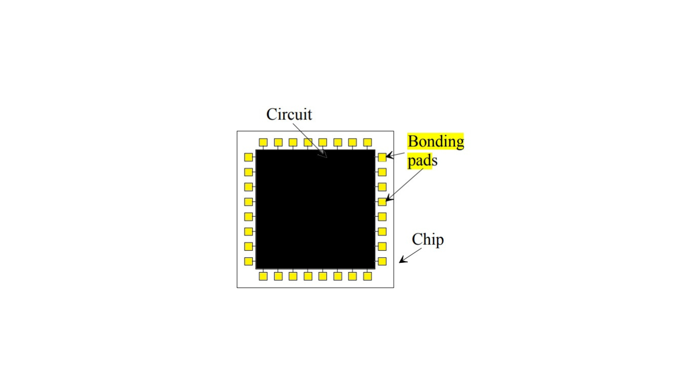
What is a Bonding Pad?
A bonding pad is a designated area on the chip’s surface, typically located along the chip boundary, that serves as a connection point for external elements, such as wires or leads, during the packaging process. These pads are crucial for establishing electrical connections between the internal circuitry of the chip and the external world, which includes connections to other components on a circuit board.
Key points about bonding pads
Package Connections
The bonding pads create a ring-like structure along the chip’s boundary, and they are specifically designed to connect the chip to the external packaging. The packaging process involves enclosing the chip in a protective package and establishing connections to the external world through these bonding pads.
Facilitating Package Connections
The bonding pads are strategically positioned to facilitate the attachment of wires or other connection mechanisms. These connections are crucial for integrating the chip into a larger electronic system.
Customization and Personalization
In the context of gate-array architectures, like the mask-programmed gate-array mentioned in the paragraph, bonding pads play a role in customizing the chip for specific applications. For example, in a gate array, designers can personalize the chip by adding metal interconnections to the existing gate cells. The bonding pads are essential for connecting these personalized elements.
Connection to FPGA (Field Programmable Gate-Array)
In the evolution of chip architectures, the paragraph mentions the introduction of Field Programmable Gate-Array (FPGA). Even in FPGAs, there are references to I/O blocks and configurable logic blocks, and bonding pads likely play a role in facilitating the external connections needed for configuring and programming the FPGA.
In summary, bonding pads are crucial elements on a chip that serve as connection points for external wiring and facilitate the integration of the chip into larger electronic systems during the packaging process.