
Charge Carriers in Semiconductors
Semiconductors are materials widely used in electronics, and they can be classified into two main types: intrinsic and extrinsic. The behavior of these semiconductors depends on the presence of impurities, which introduce mobile charge carriers.
Intrinsic Semiconductors
In intrinsic semiconductors, no impurities are intentionally introduced. These materials have their electrical properties determined solely by the inherent properties of the semiconductor material itself. In intrinsic semiconductors, the number of electrons (negative charge carriers) and holes (positive charge carriers) is equal, and they are generated by thermal excitation. This balance leads to a constant product of electron and hole concentrations, as described by the equation np = constant.
Extrinsic Semiconductors
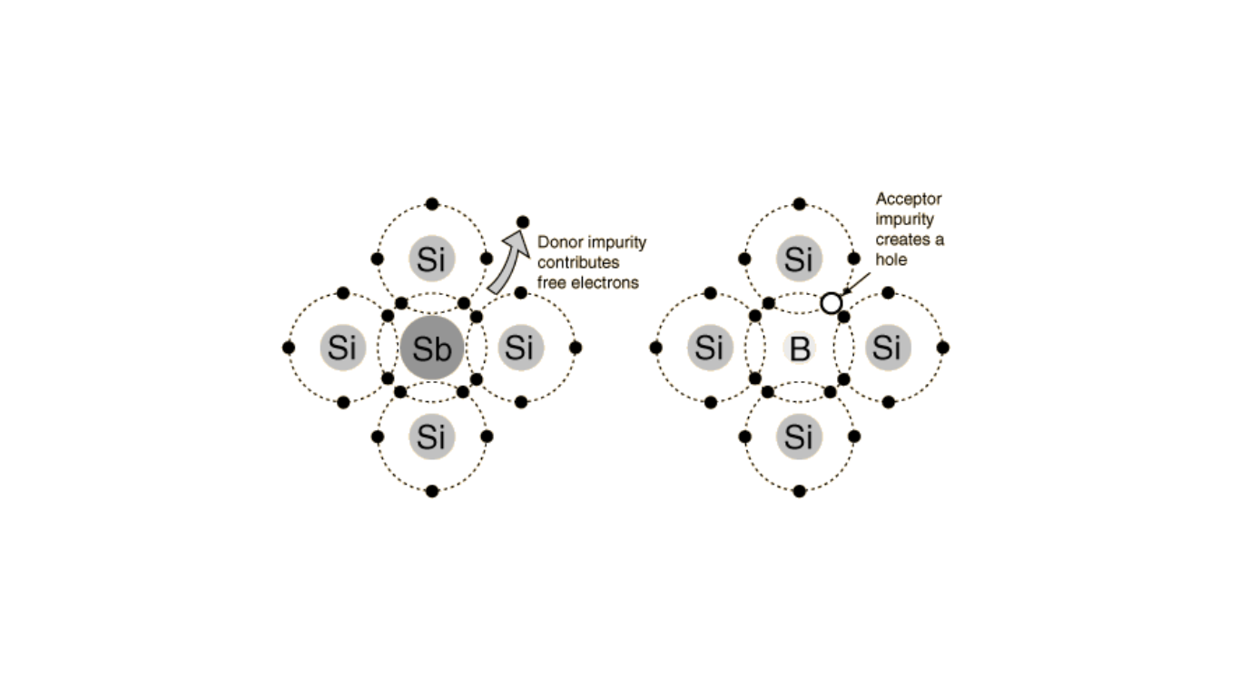
Extrinsic semiconductors are modified by introducing impurities, a process known as doping. Depending on the type of dopant used, extrinsic semiconductors can be further classified into n-type and p-type.
n-Type Semiconductor: When a pentavalent material (having five valence electrons) is introduced as a dopant into a tetravalent semiconductor material (four valence electrons), it becomes an n-type semiconductor. The pentavalent dopant provides extra electrons (negative charge carriers) to the crystal lattice, leading to an excess of electrons. This results in a higher electron concentration compared to holes.
p-Type Semiconductor: Conversely, when a trivalent material (having three valence electrons) is introduced as a dopant into a tetravalent semiconductor material, it becomes a p-type semiconductor. The trivalent dopant creates “holes” or vacancies in the crystal lattice, which act as positive charge carriers. In this case, the concentration of holes is higher than the concentration of electrons.
Negative charge carriers
Negative charge carriers in the context of electronics are electrons. These particles carry a negative charge and are liberated from their parent atoms, allowing them to move freely in space.
Positive charge carriers
On the other hand, positive charge carriers, known as holes, are charged particles that carry a positive charge. In a valence band, holes represent empty or free spaces capable of moving within the band itself. It’s essential to understand that the concept of a hole is a virtual one. When an electron relocates, it leaves behind a vacant or empty space, known as a “hole.” Since holes can accept free electrons, they are also termed acceptors.
In a semiconductor, the electron-hole pair is generated through the excitation of electrons from the valence band to the conduction band. In physics, carrier generation and recombination are the processes through which charge carriers are created and eliminated. When an electron and a hole recombine, the energy is transferred to the electron within the conduction band.
Dopants
The materials used to introduce impurities into semiconductors are called dopants. Dopants play a crucial role in tailoring the electrical properties of semiconductors for specific applications.
In summary, intrinsic semiconductors have a balanced concentration of electrons and holes due to thermal excitation. Extrinsic semiconductors, on the other hand, are intentionally doped with impurities, creating an imbalance in charge carriers and leading to n-type or p-type behavior depending on the type of dopants used. The law of mass action equation np = ni^2 is a fundamental relationship that holds true for intrinsic semiconductors.