Close Menu
  • Analog Design
    • Latest Analog Layout Interview Questions (2025)
  • Digital Design
    • Digital Electronics Interview Question(2025)
    • Top VLSI Interview Questions
  • Physical Design
    • Physical Design Interview Questions for VLSI Engineers
  • Verilog
    • Verilog Interview Questions(2024)
  • Forum
Facebook Instagram YouTube LinkedIn WhatsApp
SiliconvlsiSiliconvlsi
Ask Questions Register in Forum Login in Forum
Facebook Instagram YouTube LinkedIn WhatsApp
  • Analog Design
    • Latest Analog Layout Interview Questions (2025)
  • Digital Design
    • Digital Electronics Interview Question(2025)
    • Top VLSI Interview Questions
  • Physical Design
    • Physical Design Interview Questions for VLSI Engineers
  • Verilog
    • Verilog Interview Questions(2024)
  • Forum
SiliconvlsiSiliconvlsi
Home»Digital Design»Configurable Logic Blocks (CLBs) on an FPGA
Digital Design

Configurable Logic Blocks (CLBs) on an FPGA

siliconvlsiBy siliconvlsiJanuary 7, 2022Updated:May 28, 2024No Comments2 Mins Read
Facebook Pinterest LinkedIn Email WhatsApp
Share
Facebook Twitter LinkedIn Pinterest Email

Configurable Logic Blocks (CLBs) on an FPGA

A configurable Logic Block (CLB) is the basic repeating logic resource on an FPGA.A set of configurable logic blocks (CLBs) are used in the CLB architecture, a digital logic design, to implement Boolean functions. Many CPLD and FPGA devices use the CLB architecture. The fundamental components of the design, or logic elements (LEs), are found in various numbers within each CLB.

CLB(Configurable Logic Blocks)

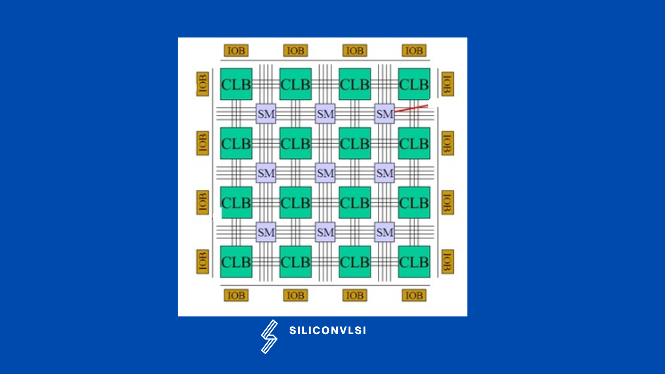
It is linked together by routing resources, the components in CLBs execute complex logic functions, implement memory functions, and also synchronize code on the FPGA. CLBs contain smaller components, include like lip-flops, look-up tables (LUTs), and multiplexers.

What is Flip-Flop?

A flip-flop is the smallest storage resource on the FPGA. and Each flip-flop in a CLB is a binary register used to save logic states between clock cycles on an FPGA circuit.

What is a Look-up Table (LUT)?

A LUT stores a predefined list of outputs for every combination of inputs. The LUTs in a CLB can also implement FIFOs and memory items in LabVIEW.LUTs provide a fast way to retrieve the output of a logic operation because possible results are stored and then referenced rather than calculated.

What is a Multiplexer?

A circuit selects between two or more inputs and then returns the selected input.

What is a slice in VLSI?

A slice is a subset of a one-dimensional array, ranging from a single element to the entire array. The prefix used for a slice is the name of the parent array. The index used for a slice must be within the range of the indexes of the parent array

Share. Facebook Twitter Pinterest LinkedIn Tumblr Email

Related Posts

Understanding the Difference Between RAM Bandwidth and Clock Speed

December 1, 2024

Why is Frequency Planning so important in Module Design?

September 2, 2024

How Are Electrostatic Discharge (ESD) Protection and Latch-Up Related to Each Other?

July 20, 2024
Leave A Reply Cancel Reply

Facebook X (Twitter) Instagram Pinterest Vimeo YouTube
  • About Us
  • Contact Us
  • Privacy Policy
© 2025 Siliconvlsi.

Type above and press Enter to search. Press Esc to cancel.