
When you look into CMOS and NMOS technology, you’ll find two major logic families in electronic circuit design. CMOS, which stands for Complementary Metal-Oxide-Semiconductor, uses both PMOS and NMOS transistors. On the other hand, NMOS, or N-channel Metal Oxide Semiconductor, relies only on FETs (Field-Effect Transistors) in its design.
CMOS Technology
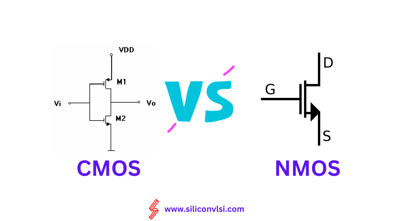
CMOS, or Complementary Metal Oxide Semiconductor, is a widely used technology in the manufacturing of ICs, digital logic circuits, microprocessors, microcontrollers, memories, and more. It combines PMOS and NMOS technologies to achieve its functionality.
CMOS technology is highly regarded in the semiconductor industry due to its low power consumption and high immunity against electronic noise. It serves as an onboard semiconductor chip powered by a battery, primarily used for data storage in computing devices. In a typical computer system, the CMOS IC maintains the system time, date, and other hardware settings.
The main advantages of CMOS devices include efficient power utilization, reduced circuit complexity, high noise immunity, minimal heat generation, and very low static power consumption. CMOS allows for high-density logic functions on a single chip. It finds applications in microprocessors, microcontrollers, memories, digital logic circuits, analog circuits such as data converters, sensors, communication devices, and more.
NMOS Technology
NMOS stands for N-channel Metal Oxide Semiconductor. NMOS utilizes N-type semiconductor material for the source and drain terminals, along with P-type semiconductor material for the substrate.
NMOS technology is used to create different microelectronic circuits found in logic chips, memory chips, and even in CMOS designs. In NMOS, there is a special layer called the N-channel layer that helps the flow of electrons between the source and drain terminals. This technology is commonly utilized in microprocessors and other metal oxide semiconductor devices because it allows for smaller chips, provides high density, and enables high-speed operation. The reason for its effectiveness is that it uses electrons as charge carriers, which have good mobility, allowing for efficient movement within the device.
Difference between CMOS and NMOS Technology
Here are the key differences between CMOS and NMOS technology:
Full form: CMOS stands for Complementary Metal Oxide Semiconductor, while NMOS stands for N-channel Metal Oxide Semiconductor.
Definition: CMOS combines both PMOS and NMOS technologies, whereas NMOS solely relies on N-type channel conduction.
Operation: CMOS utilizes symmetrical and complementary pairs of P-type and N-type MOSFETs, while NMOS creates an inversion layer within a P-type substrate for operation.
Logic level: CMOS operates with a logic level of 0 V / 5 V, whereas the logic level of NMOS depends on β ratio and noise margins.
Layout: CMOS exhibits a more regular layout, while NMOS has an irregular layout.
Power dissipation: CMOS has zero power dissipation in standby mode, while NMOS dissipates power when the output is zero.
Power supply: CMOS can operate with a power supply ranging from 1.5 V to 15 V, whereas NMOS operates with a fixed power supply depending on VDD.
Packing density: CMOS has a lower packing density, requiring 2N devices for N inputs, whereas NMOS has higher packing density, requiring (N+1) devices for N inputs.
Load-to-drive ratio: CMOS has a load/drive ratio of 1:1 or 2:1, while NMOS has a load/drive ratio of 4:1.
Transmission gate: CMOS transmission gates can pass both ‘0’ and ‘1’ logic levels effectively, whereas NMOS transmission gates can only pass ‘0’ logic well, with a voltage threshold drop for ‘1’ logic.
Static power consumption: CMOS exhibits low static power consumption, while NMOS consumes relatively more static power.
Noise immunity: CMOS has high noise immunity, whereas NMOS has comparatively lower noise immunity.
Applications: CMOS is used to design various digital logic circuits, microprocessors, microcontrollers, memories, and more. NMOS is used in the design of digital logic circuits such as microprocessors, memory chips, and other MOS devices.
In conclusion, CMOS technology is particularly well-suited for designing embedded systems. The key distinction between CMOS and NMOS lies in the lower static power consumption of CMOS compared to NMOS.