Close Menu
  • Analog Design
    • Latest Analog Layout Interview Questions (2025)
  • Digital Design
    • Digital Electronics Interview Question(2025)
    • Top VLSI Interview Questions
  • Physical Design
    • Physical Design Interview Questions for VLSI Engineers
  • Verilog
    • Verilog Interview Questions(2024)
  • Forum
Facebook Instagram YouTube LinkedIn WhatsApp
SiliconvlsiSiliconvlsi
Ask Questions Register in Forum Login in Forum
Facebook Instagram YouTube LinkedIn WhatsApp
  • Analog Design
    • Latest Analog Layout Interview Questions (2025)
  • Digital Design
    • Digital Electronics Interview Question(2025)
    • Top VLSI Interview Questions
  • Physical Design
    • Physical Design Interview Questions for VLSI Engineers
  • Verilog
    • Verilog Interview Questions(2024)
  • Forum
SiliconvlsiSiliconvlsi
Home»VLSI Design»Composite Layouts
VLSI Design

Composite Layouts

siliconvlsiBy siliconvlsiOctober 3, 2023Updated:May 19, 2024No Comments1 Min Read
Facebook Pinterest LinkedIn Email WhatsApp
Share
Facebook Twitter LinkedIn Pinterest Email

What is a Composite Layouts?

Composite layouts refer to the combination of multiple masks used in the semiconductor fabrication process to create integrated circuits. The process involves using various masks to define different features and regions on the semiconductor wafer.

Composite layouts Example

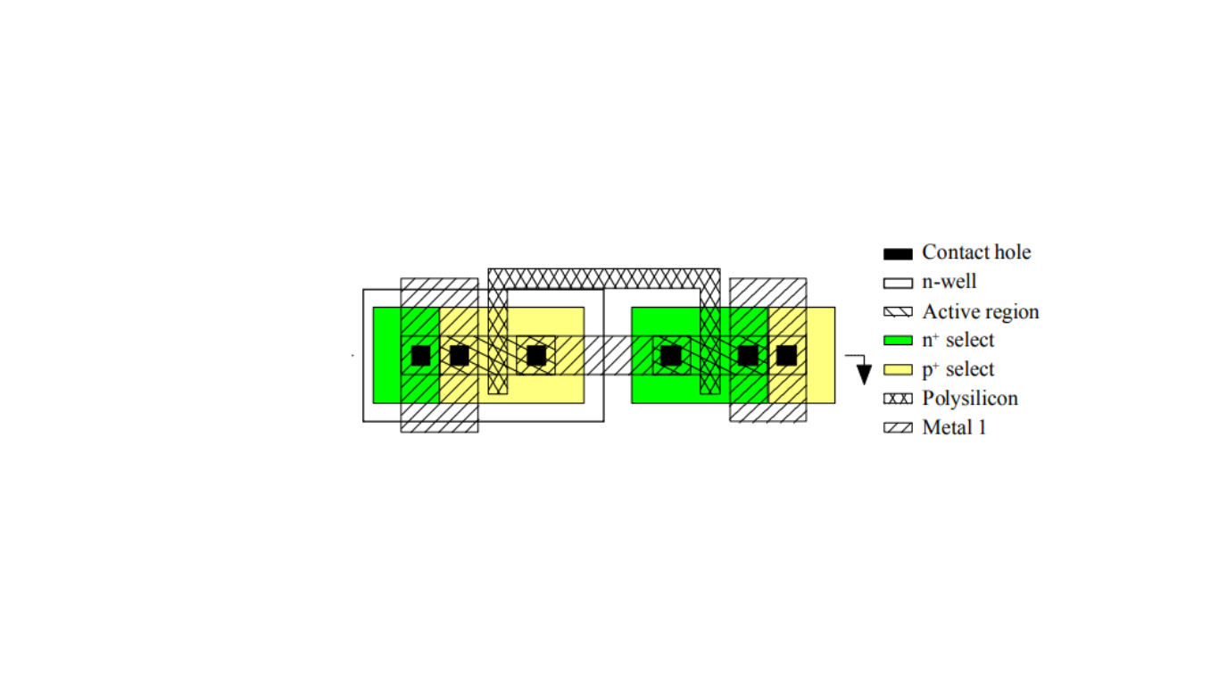
An active region mask is initially used to define the dimensions of the transistors. This mask specifies where the diffusion (i.e., source and drain regions) will take place.

A select mask is then used for the actual doping process. The openings in the select mask extend beyond the active regions, ensuring that the transistors are formed correctly.

The resulting composite layout includes the active region, select, and other necessary masks to accurately define the structure of transistors during the semiconductor manufacturing process.

The concept of composite layouts allows designers to work more conveniently with the dimensions of transistor source/drain regions while abstracting away the complexities of individual masks. Symbolic layout styles, such as the one mentioned in the context, enable designers to specify transistor properties like active regions and gates. The composite layout is then automatically generated based on these specifications and design rules.

Share. Facebook Twitter Pinterest LinkedIn Tumblr Email

Related Posts

How Shielding Avoids Crosstalk Problem? What Exactly Happens There?

September 22, 2024

Navigating the Challenges of Gate Dielectric Scaling in MOS Transistors

August 1, 2024

Challenges in Modern SoC Design Verification

April 20, 2024
Leave A Reply Cancel Reply

Facebook X (Twitter) Instagram Pinterest Vimeo YouTube
  • About Us
  • Contact Us
  • Privacy Policy
© 2025 Siliconvlsi.

Type above and press Enter to search. Press Esc to cancel.