Close Menu
  • Analog Design
    • Latest Analog Layout Interview Questions (2025)
  • Digital Design
    • Digital Electronics Interview Question(2025)
    • Top VLSI Interview Questions
  • Physical Design
    • Physical Design Interview Questions for VLSI Engineers
  • Verilog
    • Verilog Interview Questions(2024)
  • Forum
Facebook Instagram YouTube LinkedIn WhatsApp
SiliconvlsiSiliconvlsi
Forum Questions Register in Forum Login in Forum
Facebook Instagram YouTube LinkedIn WhatsApp
  • Analog Design
    • Latest Analog Layout Interview Questions (2025)
  • Digital Design
    • Digital Electronics Interview Question(2025)
    • Top VLSI Interview Questions
  • Physical Design
    • Physical Design Interview Questions for VLSI Engineers
  • Verilog
    • Verilog Interview Questions(2024)
  • Forum
SiliconvlsiSiliconvlsi
Home»Physical Design»Crosstalk and Shielding
Physical Design

Crosstalk and Shielding

siliconvlsiBy siliconvlsiOctober 15, 2022Updated:May 12, 2024No Comments2 Mins Read
Facebook Pinterest LinkedIn Email WhatsApp
Share
Facebook Twitter LinkedIn Pinterest Email

Crosstalk and Shielding

Crosstalk between the nets may severely degrade the performance of an analog circuit. thus, it is required to extract these effects during the routing. Due to crosstalk phenomena, sometimes we need to do shielding.

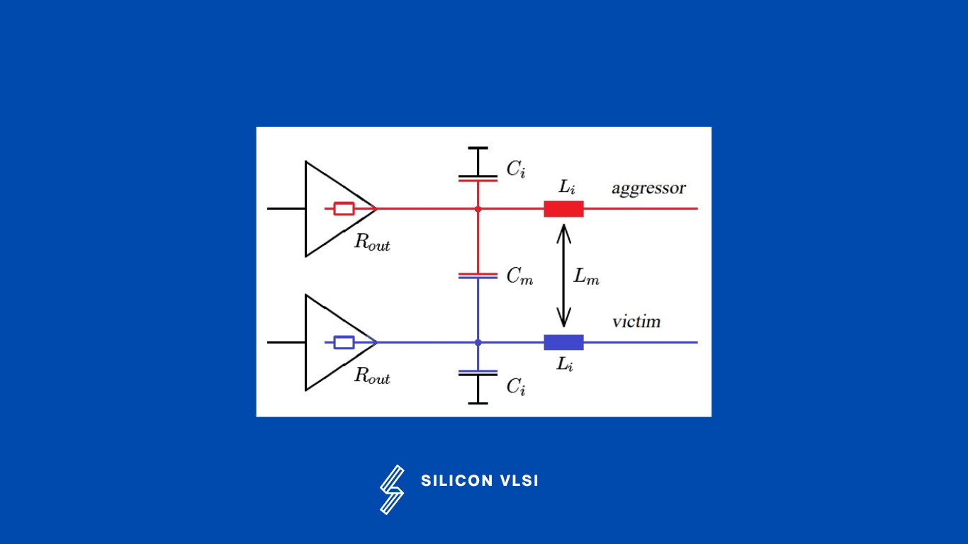
Shielding reduces crosstalk. In RF circuits, inductive coupling may also be critical for the performance and RLC models for interconnects, such as in are used to observe these inductive effects. Even EM simulations may be carried out to observe the parasitic effects more accurately

(a) Shielding on the same layer (b) Shielding between different layers (c) Shielding to avoid crosstalk through bulk

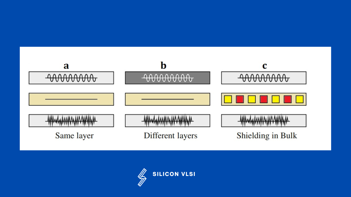
The long wires running in parallel affect the performance of the analog circuits. One way to reduce the crosstalk between these wires is to add space between them. If it is impossible to reduce the coupling by adding space, the router may introduce a shield between the critically coupled nets. To avoid the crosstalk, add a shield line between wires as shown in the above figure. In the above Figure, Three, different shielding methods are displayed. These methods may be used to reduce the crosstalk via the bulk or routing layers.

Crosstalk Prevention techniques

  • Do shielding. #
  • Increase the spacing between the aggressor and victim net.
  • Downsize the aggressor cell or Upsizing the victim cell


What is the use of shielding in VLSI?

Interconnect shielding is employed in Very Large Scale Integration (VLSI) designs to prevent noise interference among signals. This technique involves using shielding wires connected to the power supply voltage, which run adjacent to signal wires. By doing so, it mitigates signal switching-induced noise through cross-coupling capacitance to neighboring signals.


Share. Facebook Twitter Pinterest LinkedIn Tumblr Email

Related Posts

Why Are Metals Good Conductors of Electricity?

November 21, 2024

Difference between Mesh Topology and Tree Topology

March 24, 2024

What’s the difference between Design Rule Check (DRC) and Design for Manufacturability (DFM)?

October 26, 2023
Leave A Reply Cancel Reply

Facebook X (Twitter) Instagram Pinterest Vimeo YouTube
  • About Us
  • Contact Us
  • Privacy Policy
© 2025 Siliconvlsi.

Type above and press Enter to search. Press Esc to cancel.