
Dummy Device in Semiconductor Layout Design
In precision analog circuit design, achieving consistent and accurate matching between devices is crucial for reliable performance. However, variations in the fabrication process and local inhomogeneities near the boundary of matching groups can lead to mismatches. To address these issues, dummy elements are strategically placed in layouts. Let’s explore the concept and rules of thumb regarding dummy elements:
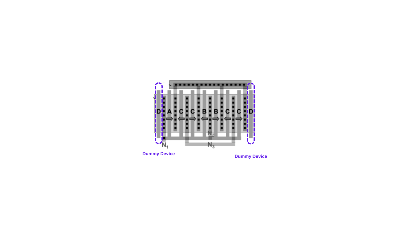
Purpose of Dummy Elements
Dummy elements are non-functional, identical structures placed in close proximity to actual devices within a matching group.
Their primary purpose is to ensure that devices within the matching group experience the same “neighborhood conditions,” both inside and at the group’s edges.
Addressing Local Inhomogeneities
Local inhomogeneities can arise due to variations in fabrication steps or neighboring structures. For example, adjacent features might require stronger or weaker etching, leading to changes in device properties.
Dummy elements help maintain uniform neighborhood conditions for devices in the matching group, minimizing the impact of such local variations.
Use Cases for Dummy Elements
Dummy elements are placed at both sides in layout versions to create consistent surroundings for devices.
In matched resistor series, dummies are positioned at the beginning and end.
Two-dimensional capacitor arrays are entirely surrounded by dummies, although this consumes additional space.
Well Proximity Effect (WPE)
WPE is a known issue where higher dopant concentrations occur approximately 1 µm from the boundary of wells due to scattering during well implantation.
This effect can significantly alter the threshold voltage (Vth) of MOS-FETs, leading to mismatches.
Placing matching elements at a safe distance from the well boundary helps avoid WPE-induced mismatches.
Trench-Isolation Stress(STI)
Trench-isolation stress is not caused by fabrication tolerances but results from mechanical pressure exerted by trench isolations on adjacent silicon.
This pressure, which depends on temperature variations, can impact carrier mobility, affecting device behavior.
Dummy elements can also help counteract stress caused by shallow and deep trench isolations (STI, DTI).
Rules of Thumb
Maintain consistent neighborhood conditions both inside and at the edge of matching groups by surrounding the group with the same dummy elements as inside.
To avoid the well proximity effect (WPE), place matching elements at a safe distance from the well boundary.
Incorporate dummy elements as a standard measure to counteract stress induced by shallow and deep trench isolations (STI, DTI).
In summary, dummy elements play a critical role in achieving precise device matching by ensuring that devices within a matching group experience uniform surroundings. They help mitigate the impact of local variations, well proximity effects, and trench-isolation stress, ultimately leading to more reliable and predictable circuit performance.