
Dynamic CMOS Logic
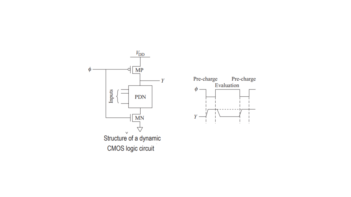
Dynamic CMOS logic is quite similar to pseudo-nMOS logic but includes an additional nMOS transistor (MN) connected between the pull-down network and the ground. Both the pMOS transistor in the pull-up network (PUN) and the extra nMOS transistors in the pull-down network (PDN) are controlled by a clock signal (φ), as depicted in Figure 1
In static CMOS logic, the pull-up network, typically implemented using pMOS transistors, can be considered somewhat redundant since the pull-down network (nMOS transistors) alone is sufficient to achieve the desired functionality. To reduce the number of transistors and improve efficiency, pseudo-nMOS logic is introduced. In pseudo-nMOS logic, the pull-up network is replaced by a single pMOS transistor with its gate terminal connected to the ground. However, it’s worth noting that pseudo-nMOS logic suffers from a significant drawback, which is substantial static power dissipation.
Dynamic CMOS logic operates in two phases during a single clock pulse (φ):
Pre-Charge Phase (φ = 0): In this phase, the output is pre-charged to a logic high level.
Evaluation Phase (φ = 1): In this phase, the output is evaluated based on the applied input logic conditions.
Advantages of Dynamic Logic Circuits
- Low Power Dissipation: They consume less power.
- Small Area: They require fewer transistors, resulting in a smaller physical footprint.
- Large Noise Margin: They exhibit a higher tolerance for noise.
However, dynamic CMOS logic circuits face a significant challenge when cascaded. In the pre-charge phase (φ = 0), the outputs of all stages are pre-charged to logic high. In the evaluation phase (φ = 1), the outputs of all stages are evaluated simultaneously. Here’s where the problem arises: if the inputs in the first stage lead to a logic low output after evaluation, and the subsequent stages have inputs that discharge their outputs to logic low, then the evaluated output of the first stage can never make the output of the second stage go logic high. This is because the evaluation occurs simultaneously, and the output can only be retained in logic high, not charged to it, during the evaluation phase (φ = 1).