
Electron-Beam Lithography (EBL)
Electron beam lithography (EBL) is a powerful direct-write method that you and I can use when we need to create extremely precise patterns on a surface. Instead of using light like in traditional lithography, we rely on a finely focused beam of electrons to draw custom designs directly onto the substrate. This technique is especially useful when we’re working at the nanoscale and need high-resolution results that standard photolithography can’t achieve.
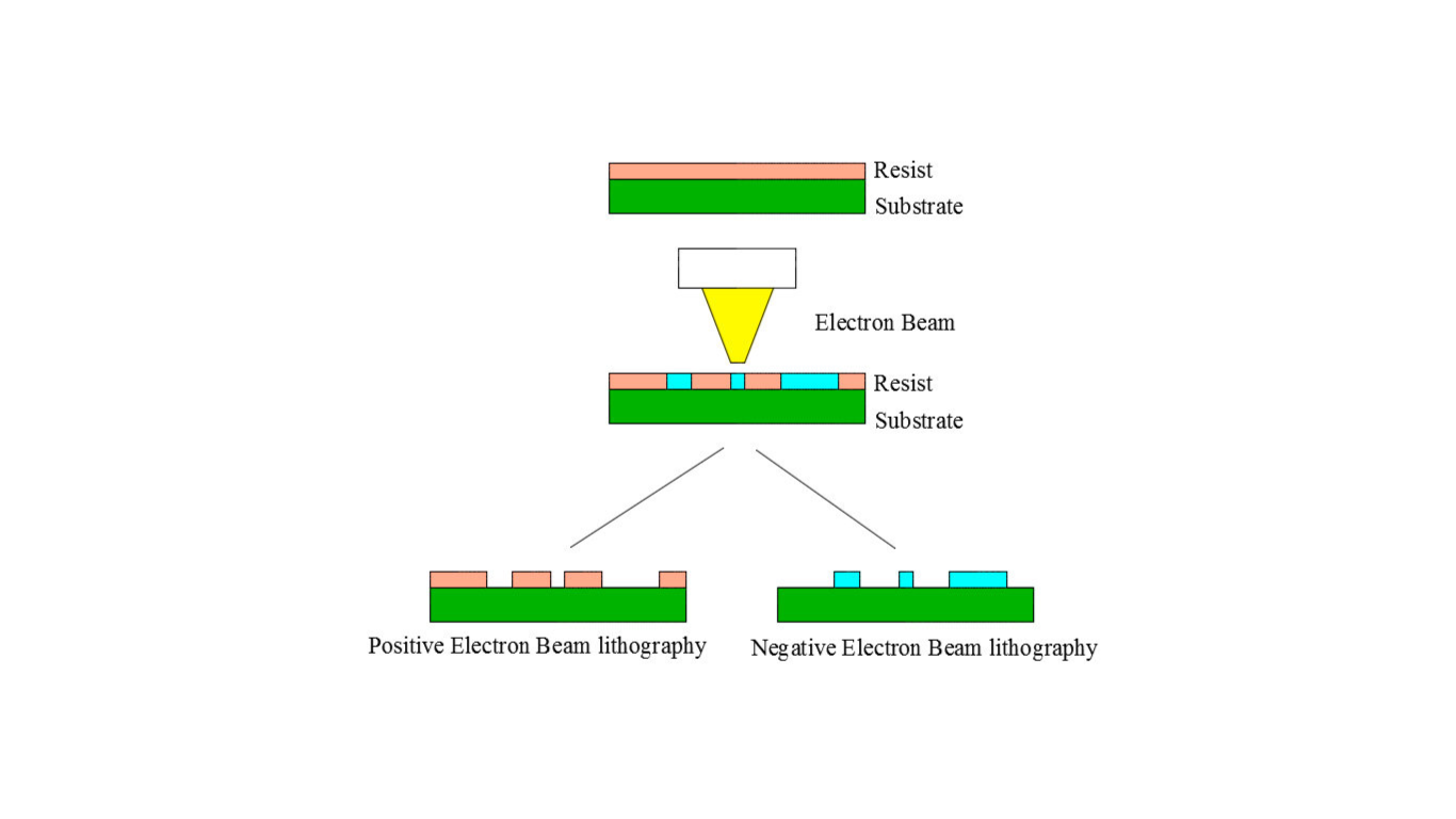
When you use electron-beam lithography (EBL), you’ll be scanning a focused beam of electrons to create custom shapes on an electron-sensitive resist film. The electron beam changes the resist’s solubility, allowing us to selectively remove either the exposed or unexposed areas of the resist by immersing it in a solvent.
The primary advantage of EBL is its ability to draw custom patterns with sub-10 nm resolution, which we call direct-write capability. However, you’ll find that EBL has a significant drawback due to its low throughput. The time required for writing is relatively high, making us question its feasibility as a lithography tool in future technology roadmaps.
High Resolution Lithography Technique
E-beam resists come in two varieties, Positive Electron Beam and Negative Electron Beam, similar to optical lithography. Positive Electron Beam resists developing away at exposed parts, but negative Electron Beam resists leaving the developed region behind after development.
One limitation of EBL is observed when patterning small features. To achieve this, the number of electrons in the beam must be reduced, leading to a large change in dose due to shot noise effects.
The new generation of EBL addresses some of these issues by employing secondary electrons as the main beam. When high-energy electrons interact with atoms, they can pull out electrons from the atom’s shell, inducing a secondary electron beam. These secondary electrons have significantly lower energy and cause fewer beam-related defects.
In conclusion, EBL offers the advantage of high-resolution direct-write capability, enabling custom patterns with sub-10 nm resolution. However, it’s low throughput and challenges with dose variation for small features have raised doubts about its suitability as a lithography tool in future technology advancements. The use of secondary electrons in the new generation of EBL shows promise in mitigating some of these issues and improving the performance of the technique.