
Enhancement-type nMOS
MOS (Metal-Oxide-Semiconductor) inverter that uses an enhancement-type nMOS (n-type Metal-Oxide-Semiconductor) transistor as a load instead of a resistive load. This design helps overcome some of the drawbacks of a resistive inverter but introduces other challenges.
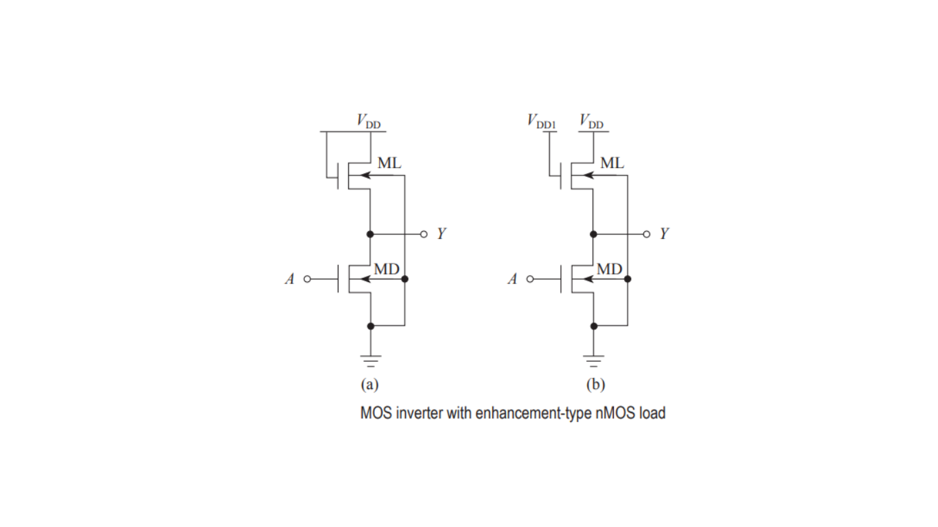
Alternative MOS Inverter Design with nMOS Transistor Load
In this design, MOS inverter uses an enhancement-type nMOS transistor (referred to as ML) as its load, as illustrated in Figure 1
Load Transistor Operation
The load nMOS transistor ML can operate in two different modes:
Saturation Region: In Figure 1(a), ML operates in the saturation region. Here, its gate and drain are shorted together and connected to the power supply voltage VDD.
Linear Region: In Figure 1(b), ML operates in the linear region, depending on the bias voltage VDD1.
Enhancement-type nMOS Operation
When the input to the inverter is at logic low, the driver nMOS transistor MD is turned OFF. In this state, the output is at logic high through the load transistor ML.
Conversely, when the input is at logic high, the driver nMOS transistor MD turns ON, connecting the output to ground through MD.
Enhancement-type nMOS Drawbacks
While this alternative design can mitigate some of the drawbacks of using a resistive load, it introduces its own challenges, such as the need for dual power supply voltages. Having both configurations, as shown in Figure 3.6, can result in significant static power dissipation.
In summary, this design variation of the MOS inverter uses an enhancement-type nMOS transistor as a load, offering advantages over resistive loads in terms of area efficiency. However, it also comes with its own set of challenges, including the requirement for dual power supplies and the issue of static power dissipation.