Gate Oxide
Achieving thinner gate oxide or larger gate capacitance per unit area is crucial for enhancing both off-state and on-state device characteristics. In advanced technology, gate oxide thickness has been scaled down to below 20 angstroms, often incorporating nitridation processes to enhance resistance against dopant penetration. However, in such ultra-thin SiO2 layers, direct-tunneling gate leakage becomes a significant factor, even at reduced power supply voltages. This results in substantial off-state power consumption issues.

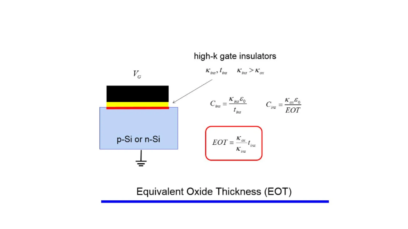
Equivalent Oxide Thickness (EOT)
To address this challenge, high-κ gate dielectrics have been explored as a potential solution. These materials can achieve a given equivalent oxide thickness (EOT) while having a physically thicker layer compared to SiO2. Yet, challenges related to high-κ gate dielectrics, such as mobility degradation and flat-band voltage shift, are still under investigation.
Handling gate leakage current problems requires not only technological advancements but also circuit and system-level techniques. Tailoring process technologies to match design requirements based on application types, such as high-performance, low-power, and standby-power applications, is also beneficial.
Linked to gate dielectric EOT scaling is the polysilicon gate depletion effect. When devices are turned on, a thin depletion layer (approximately 1 nm) forms in the polysilicon gate due to its doping concentration. This layer weakens the capacitive coupling between the gate and the channel, ultimately reducing the effective gate overdrive voltage. As gate dielectric EOT approaches 1 nm, the impact of the gate depletion layer becomes significant. While increasing active doping concentration in the gate helps, a more complete solution involves adopting metallic gate electrodes.
Quantum-Mechanical Effects
Additionally, quantum-mechanical effects in the channel introduce an extra capacitance in series with the gate oxide capacitance. In contemporary and future CMOS devices with sufficiently high vertical electric fields, carrier movement in the channel becomes confined in a potential well. This leads to discrete energy states instead of a continuous spectrum. Consequently, the peak of the carrier distribution shifts closer to the substrate-oxide interface, contributing a few angstroms to the gate dielectric EOT.
Similar to the polysilicon gate depletion effect, this quantum effect was relatively insignificant until sub-100-nm technology generations. The magnitude of the quantum effect is influenced by factors such as vertical field, substrate doping, and silicon body thickness in ultrathin body MOSFETs. It’s important to recognize that this is a fundamental physical limit that cannot be solely resolved through process enhancements.
Process Variations
Process variations are a critical concern in design, particularly as device scaling progresses. Variations in key device parameters, such as the threshold voltage (Vth), become more pronounced. Key sources of variations include fluctuations in dopant concentration, variations in oxide thickness, critical dimension (CD) fluctuations, and line edge roughness, among others.
As devices become smaller, the total number of dopants in the channel decreases, leading to increased statistical fluctuation. This increase follows a trend of 1/N^1/2, where N represents the number of dopants. While the specific impact on Vth variation depends on the doping profile, this overall trend is unfavorable for device scaling. Innovative device structures, like the double-gate MOSFET, which require minimal doping concentration in the channel, can be employed to mitigate this issue. However, these devices may be sensitive to other sources of variation, such as silicon body thickness.
With reduced device dimensions, the tolerance for variations in critical dimensions and film thickness also diminishes. Consequently, the need for more robust design methodologies becomes paramount. These methodologies, in conjunction with process enhancements, are essential for achieving improved yield and performance in the face of increasing process variations.