
ESD Protection Scheme
The concept of on-chip ESD protection design, as depicted in the accompanying figure, is employed to prevent damage caused by the Human Body Model (HBM) and Machine Model (MM) ESD stresses, which occur with nearly arbitrary combinations of pins. Each input or output pin is equipped with ESD clamp devices positioned between the pad and the VDD (supply voltage) and VSS (ground) power lines. These clamp devices serve to dissipate the four different modes of ESD stresses that can affect the I/O pin.
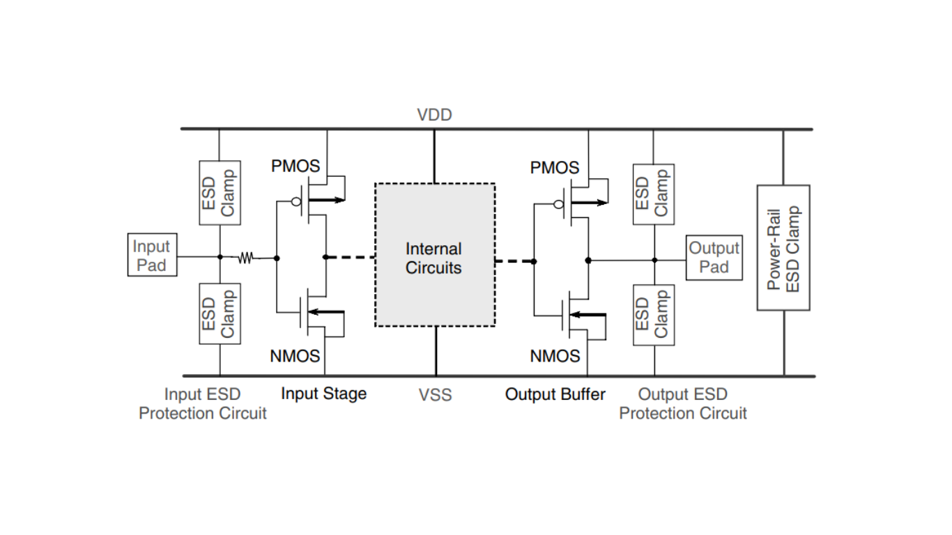
To effectively mitigate ESD stresses arising from pin-to-pin interactions and from voltage supply rail differences (VDD-to-VSS), it is essential to include power-rail ESD clamp circuits positioned between the VDD and VSS power lines of the integrated circuit. In many logic ICs, the power pins for I/O circuits are deliberately segregated from the power pins of the core circuits. This separation serves a dual purpose: it helps prevent issues related to noise coupling and contributes to the reduction of ground bounce phenomena.
ESD Protection Guidelines
Here are some guidelines for designing ESD (Electrostatic Discharge) clamp devices or circuits for I/O pins or power pins:
Efficient ESD Protection Scheme: Provide the integrated circuit (IC) with an effective ESD protection scheme that can divert any ESD stress away from the IC during ESD stress conditions.
Signal Passing and Inactivity: Allow normal I/O signals to pass through the protection circuit while ensuring that the circuit remains inactive during the IC’s regular operation.
Reduced Input Capacitance and Resistance: Minimize the input capacitance and resistance to ensure acceptable I/O signal delay while maintaining signal integrity.
High ESD Robustness in Compact Layout: Design the ESD protection circuit to have a high level of robustness against ESD events while keeping the layout area reasonably small.
Latch-Up Immunity: Maintain a strong latch-up immunity in CMOS ICs by surrounding all I/O devices and ESD protection devices with guard rings. The fabrication of these ESD protection devices should ideally be compatible with the existing process technology, avoiding the need for additional mask layers or process modifications if possible.
Non-Interference with Functionality: Ensure that the ESD protection circuits do not interfere with the normal functionality of I/O circuits during regular operation. This is particularly important for applications that involve high-voltage-tolerant I/O or power-down operations.