The channel between the source and drain in fin MOSFETs is constructed as a three-dimensional bar on top of the silicon substrate, in contrast to planar MOSFETs. The channel is then wrapped in the gate electrode, creating several gate electrodes on each side, which reduces leakage effects and improves driving current.
FinFET Fabrication Steps
Wafer preparation
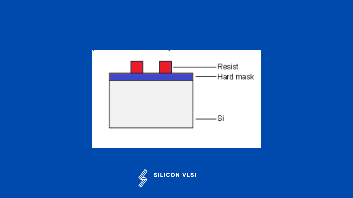
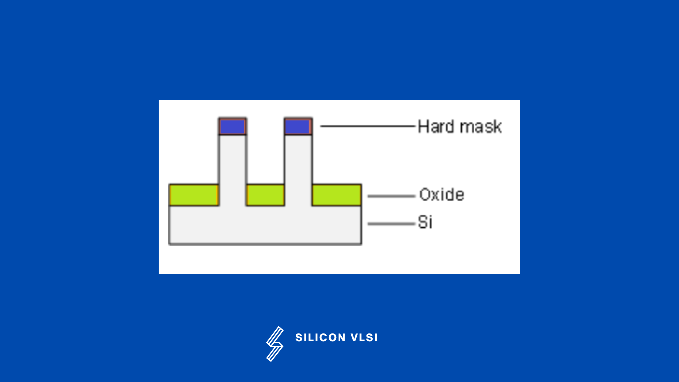
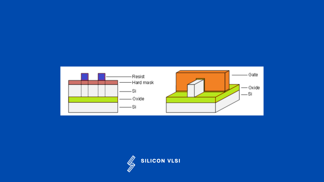
The first step in the FinFET fabrication process is to prepare the wafer that will be used to create the transistors. This typically involves cleaning the wafer and applying a layer of oxide to the surface. The basis for a FinFET is a lightly p-doped substrate with a hard mask on top (e.g. silicon nitride) as well as a patterned resist layer. #
Fin etch
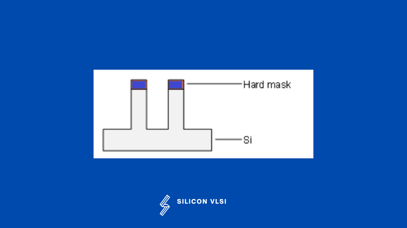
In a highly anisotropic etch process, the fins are created. Since a bulk wafer lacks a stop layer as an SOI wafer does, the etch process must be time-based. The fins’ breadth in a 22 nm process could be between 10 and 15 nm, but they should ideally be twice that height or larger. #
Oxide deposition
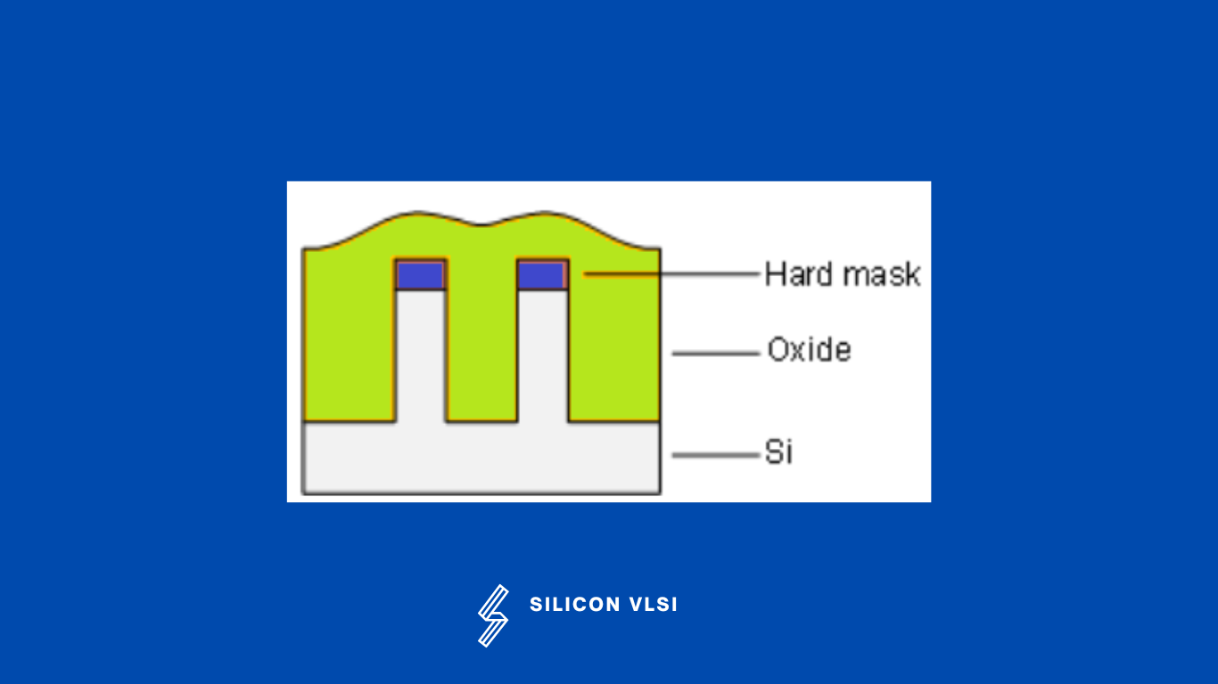
The next step is to deposit various layers of material onto the wafer, using techniques such as chemical vapor deposition (CVD) or physical vapor deposition (PVD). These layers include the gate dielectric, the gate electrode, and the source and drain regions.#
Planarization
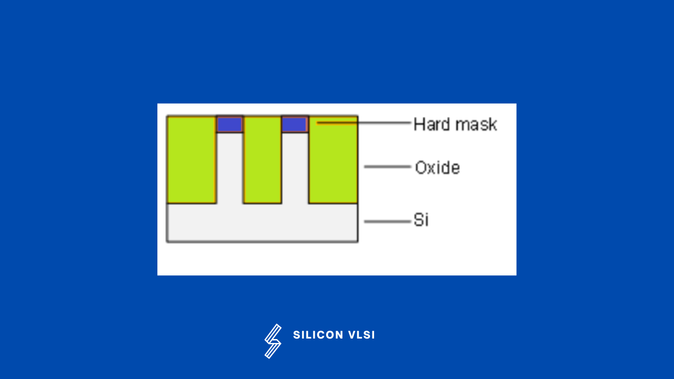
Planarization is the process of increasing the flatness or planarity of the surface of a semiconductor wafer through various methods like Chemical Mechanical Polishing(CMP) known as planarization techniques. The starting raw wafers for semiconductor device fabrication are ideally flat or planar. #
Recess etch
A recess is disposed of at least in the first layer. Also described is a method of forming a semiconductor structure that includes a recess. #
Gate oxide
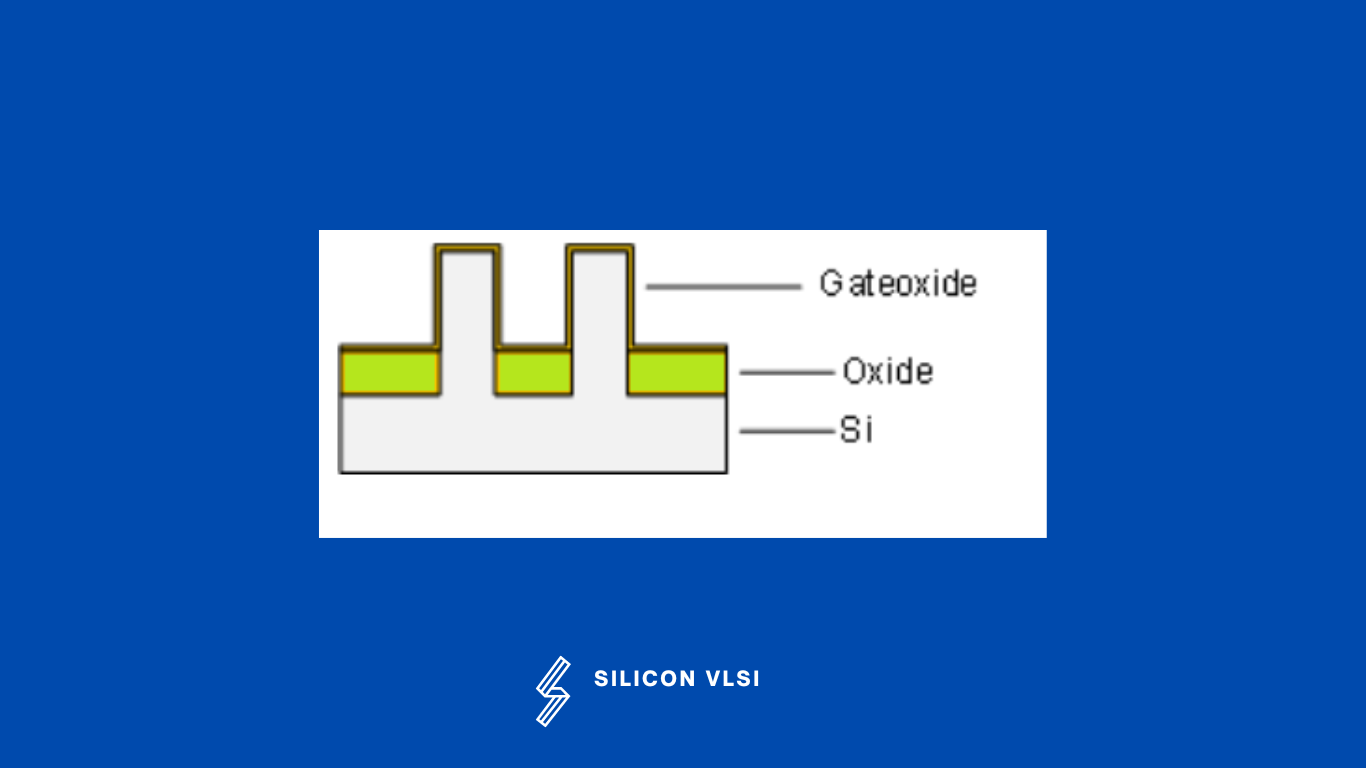
To separate the channel from the gate electrode, the gate oxide is thermally oxidized and then placed on top of the fins. A high-dose angled implant at the base of the fin establishes a dopant junction and completes the isolation because the fins are still connected underneath the oxide. #
Deposition of the gate
Last but not least, a highly n+-doped polysilicon layer is deposited on top of the fins. As a result, up to three gates—one on either side of each fin and—depending on the thickness of the gate oxide on top—a third gate above—are wrapped around the channel. #
What are some of the advantages of FinFETs over advanced planar transistors?
FinFETs offer several advantages, including lower leakage current, higher speeds, lower operating voltage (VDD), reduced power consumption, and improved scaling capabilities.
What are some of the drawbacks associated with the processing of FinFETs?
The processing of FinFETs is more complex and costly compared to planar devices. This complexity arises from the three-dimensional channel structure and the need to create a well-behaved gate stack on the fin. Forming low-contact resistance source/drains also adds significant complexity.
How is the silicon fin etching process in a silicon-on-insulator (SOI) FinFET process different from traditional silicon fin etching?
In an SOI FinFET process, the silicon fin etch is not timed because the underlying buried oxide (BOX) layer serves as an etch stop. The goal of the fin etch process is to create uniform width and height fins, with heights typically being twice or more the width.
What is the purpose of shallow trench isolation (STI) in FinFET technology, and how is it achieved?
STI is used to isolate adjacent devices from each other and to isolate local overlying interconnects from the substrate. To achieve STI, a sequence of steps involves depositing CVD oxide to fill trenches formed by the fins, planarizing with chemical mechanical polishing (CMP), and then etching to expose the sidewalls of the fins.
Could you describe the key steps involved in forming the patterned gate stack in FinFET fabrication?
The gate stack formation begins with the deposition of a high-quality oxide on the exposed surfaces of the fins, serving as the gate dielectric. This is followed by the deposition of a gate electrode material, such as polysilicon. Once the gate stack is formed, it undergoes a controlled etch process to pattern the gate. A hard mask protects the fins during this gate etching process.