
A survey on VLSI Floorplanning
Floorplanning helps to determine the locations, shape, and size of modules in a chip, and as such it estimates the chip area, delay, and wiring congestion, thereby providing a groundwork for layout.
Your Floorplan determines the quality of your chip. A well-organized floor plan allows for more efficient use of the core area, facilitating the placement of standard cells. while avoiding concerns such as congestion, timing, and signal integrity.
If the floorplan is bad, it impacts the chip’s area, power, and reliability, and it necessitates more work for closure, which can raise the entire IC cost. It can cause a variety of problems in the design, such as congestion, time, noise, IR, and routing issues.
Inputs for Floorplanning
- Netlist (.spi or .siz or .cir)
- Technology file (.tf)
- Timing Library files (.lib)
- Physical library (.lef)
Floorplanning Goals
- Decide the location and number of power pads.
- Assign the shape and location of Blocks
- Help to decide the location of 1/0 pads.
- Help to decide the type of power distribution.
- Decide location and type of clock distribution
Advantage oF Floorplanning
- Minimize chip area(low cost).
- Minimize delays (higher frequency).
- Keep blocks physically close to each other.
- Minimize wire length.
Floorplanning Helps to follow Factors
- To determine to aspect ratio
- Congestion and Routing issue
- IR Drop
- Timing
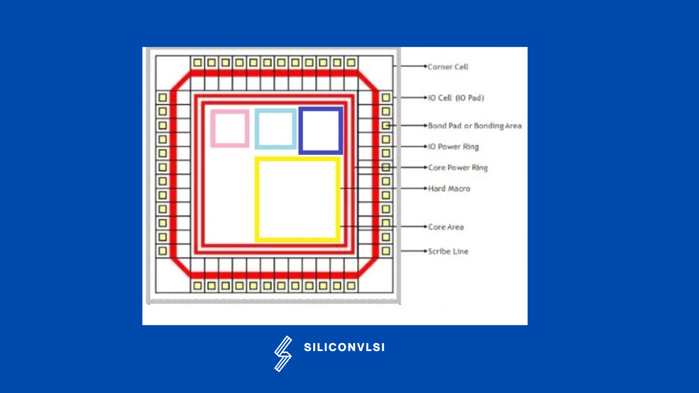
Different Types of Blockage
Soft Blockage: It prevents standard cells from being inserted inside the blockage area and permits buffers to be placed during optimization to meet timing requirements.
Hard Blockage: Inside the hard lockage area, both standard cells and buffers are not allowed.
Partial Blockage: The designer can choose how much space is available inside the blockage area. When a value of 50% is specified, 50% of the area is blocked for any placement and the remaining 50% is open for optimization.
What is Hierarchical Floorplanning?
For handling huge designs, a hierarchical floorplanning design process is an effective way. Different design teams can work on each block in parallel by breaking the design into many blocks. Working with smaller blocks and employing multiply-instantiated blocks can minimize total runtime. To split the design into blocks, produce hierarchical physical design constraints, and distribute top-level temporal budgets to lower-level physical blocks, design planning is accomplished during the first step of the hierarchical flow.
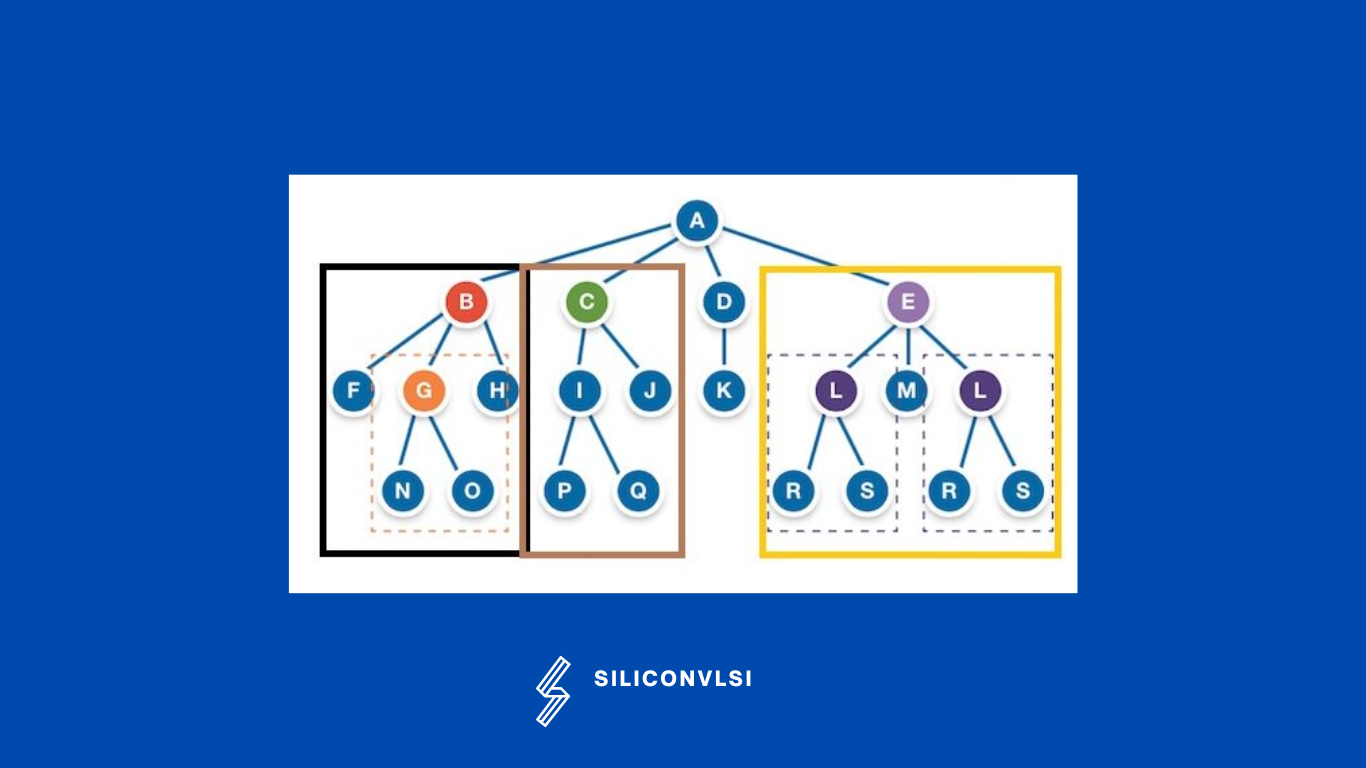
Hierarchical Floorplan Advantages:
- Faster runtime, less memory needed
- Ability to do design re-use
- Faster eco turn-around time
Hierarchical Design Floorplan Disadvantages:
- Full chip timing closure is much more challenging.
- More thorough design planning is required.
- Timing constraint budgeting
- Repeater insertion and feed through the creation
Floorplanning and Powerplannig are necessary for Physical design
Objectives of Floorplan
The objectives of floorplanning in integrated circuit design are as follows:
Minimize Area: The primary objective is to minimize the physical area occupied by the components and interconnections on the chip.
Minimize Timing: Another goal is to minimize the time it takes for signals to propagate through the chip, ensuring efficient operation and faster performance.
Reduce Wire Length: Floorplanning aims to reduce the length of interconnecting wires between components, which helps improve signal integrity and reduces signal delay.
Ease of Routing: A well-designed floorplan makes routing connections between components easier and more efficient, leading to simpler and more robust layout designs.
Reduce IR Drop: Floorplanning also considers reducing voltage drops (IR drop) across the chip’s power distribution network, ensuring stable and reliable power supply to all components.
Overall, floorplanning plays a crucial role in optimizing the layout and design of integrated circuits to meet various performance, area, and reliability requirements.