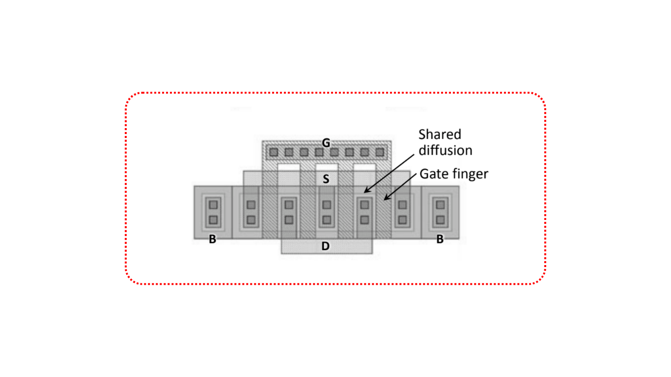
Folding the Transistors
Folding FETs in electronic circuits is done to address layout and aspect ratio considerations. When FETs have very large width-to-length (w/l) ratios, which is often the case for high-current or low-resistance applications, the aspect ratio of the transistor can become unfavorable. Folding allows the transistor to be split into multiple subtransistors with smaller widths, which collectively achieve the desired width while maintaining a more compact layout.

Folding Concept in Layout
To solve this issue, engineers use a technique called “folding.” Here’s how it works:
Splitting Into Subtransistors: Imagine you have a single FET with a wide channel but a relatively short length. When you fold it, you split it into several equal sub-transistors, each with the same length but a smaller width. These subtransistors are like smaller building blocks of the original FET.
Flipping and Sharing: Now, take two of these subtransistors and flip them so that their source and drain regions face each other. Since these regions are always at the same electrical potential, they can be shared by the subtransistors. It’s like stacking them on top of each other.
Compact Configuration: This folding process results in a much more compact configuration. The contacts for these subtransistors are now arranged in parallel, which is more space-efficient.
The layout you see at the end is a visual representation of this folded FET, and it’s not how it’s actually manufactured. In practice, specialized software generates these layouts based on the desired parameters, including the number of folds.
The “fingers” you mentioned are essentially the individual subtransistors created through folding. They get their name because they often have a finger-like shape. It’s important to note that when someone talks about the “width” of a poly finger, they are referring to the “length” of the channel, which is where the current flows.
Folding offers several advantages, including reducing gate resistance (the resistance encountered when charging and discharging the gate) and making more efficient use of space on the semiconductor wafer. It’s a common technique in semiconductor layout design to optimize the performance and size of FETs.
How is a folded FET constructed in terms of subtransistors?
A folded FET is constructed by splitting the original transistor into ‘n’ equal subtransistors, all having the same length (l) but a reduced width (w/n). These subtransistors are then shunted or connected in parallel to achieve the required total width (w) of the original transistor. This configuration helps in maintaining the desired width while reducing the aspect ratio of the individual subtransistors.
Can you explain the steps involved in folding a FET with an example?
Let’s consider an example of folding an NMOS-FET with a width (w) of 20 and a length (l) of 2, using ‘n’ equal subtransistors where n = 4:
Splitting: The NMOS-FET is divided into four imaginary subtransistors, each having a width of w/4 = 5 (step 1). Each of these subtransistors contains four vias, determined by design rules.
Flipping: Two of these imaginary subtransistors are flipped so that their respective sources and drains are facing each other (step 2). This is done because these regions are always at the same potential.
Sharing: The regions with sources and drains facing each other are virtually pushed on top of each other (step 3). This results in a compact configuration where these regions are shared by the subtransistors.
Layout Configuration: The layout is configured so that the contacts are routed as a parallel circuit (step 4).
It’s important to note that this example illustrates the internal composition of a folded FET, and in practice, layout generation tools are used to create the folded layout efficiently.
What are some advantages of folding transistors in integrated circuit design?
Folding transistors in integrated circuit design offers several advantages:
Improved Aspect Ratio: Folding allows for a more favorable aspect ratio in the layout, which can be crucial for achieving desired electrical characteristics.
Compact Layout: The folded configuration results in a more compact layout, saving valuable chip area.
Reduced Gate Resistance: Folding reduces the gate resistance of the transistors, which can be advantageous for high-speed and low-power applications.
Minimized Parasitics: Folding can help minimize parasitic capacitance and resistance, improving overall circuit performance.
Uniform Current Distribution: By connecting source and drain terminals with multiple contacts, folding ensures a uniform and efficient routing of source-drain current, minimizing parasitic resistance (RDS).
Overall, folding is a valuable technique in IC design, especially when dealing with transistors requiring high current or low resistance.