
Full Custom Layout Design Style in ASICs
A full custom ASIC is a custom-designed integrated circuit where every component is individually inserted in both design and layout. This design style offers maximum design freedom, enabling optimal performance, size, and power consumption. It stands out for its specific cell layout and the use of specific masks for manufacturing.
The full custom design style in Application Specific Integrated Circuits (ASICs) represents the most customized and specific approach to designing and manufacturing integrated circuits. In this style, every component of the ASIC is individually designed and laid out. This level of design freedom allows for optimal performance, size, and power consumption, making it ideal for applications where maximum optimization is required. Here are some key characteristics of the full custom design style:
Full Custom Layout Design Advantage
- Maximum Design Freedom: Full custom ASIC design provides designers with the utmost freedom to craft every aspect of the circuit. This includes the individual layout of components, allowing for flexible and optimized forms.
- Specific Masks: In full custom ASIC design, all masks used in the manufacturing process are specific to the particular design, leaving no room for generic or off-the-shelf components.
- Optimal Performance: One of the primary advantages of the full custom style is the potential for achieving optimal performance in terms of speed, power consumption, and functionality.
- High Component Density: Custom layouts enable high component density on the chip, making it possible to integrate a large number of parts effectively.
- Economical for High Volume: Full custom design styles are most economical when producing a high volume of parts, as the initial design effort can be justified by mass production.
Full Custom Layout Design Disadvantage
However, the full custom design style has its drawbacks:
- High Design Effort: The design process for full custom ASICs is associated with high effort, both in terms of time and cost. Each component must be meticulously designed, which can be time-consuming.
- Design Risk: Since full custom designs often rely on untested or proprietary cells, there can be a higher design risk compared to using standardized components.
Designing and laying out a full custom ASIC requires a significant amount of experience and expertise, making it most common in mixed-signal and analog applications where precise control over performance is essential.
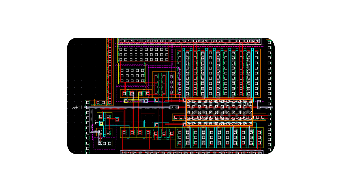
As an example, consider an ASIC designed for the direct conversion of digital satellite TV signals. The block diagram shows that it involves amplification, signal mixing, oscillator signal generation, and phase synchronization. This ASIC operates in a wide frequency range and demands high linearity and tuning capabilities.
The layout of such a direct conversion ASIC, shown in Figure q, illustrates the individual cell outlines typical of full custom design. Achieving this layout requires extensive experience, as it is challenging to meet stringent specifications concerning cross-talk and quadrature deviation. While the design is entirely customized, some repeating cells can still be identified, demonstrating the complexity of the layout. Experience gained from previous designs plays a crucial role in achieving success in full custom ASIC design.
Standard Cell Design Style in ASICs
A standard cell represents a pre-defined logic block that typically embodies a low-complexity logic function, such as NAND, NOR, or FlipFlop. Standard cells are designed, tested, and optimized to be used as building blocks in ASIC design.
How are standard cells typically organized and arranged in ASIC layouts?
Standard cells are usually organized in rows, with power supply lines running above and below the logic circuits. These cells are designed to have a uniform height and are often placed in rows with “running through” supply lines for a convenient layout.
What is the main advantage of using standard cells in ASIC design?
One of the main advantages of standard cells is the significant reduction in design time. They offer a shorter design cycle compared to full custom design. Additionally, standard cells are economical for designs with a moderate number of parts and carry a lower design risk due to their use of a tested library.
What is a potential disadvantage of standard cell design?
In cases with a small number of parts, standard cell design can become uneconomical because it requires the production of specific masks for each design. Additionally, the sub-optimal performance of transistors, which cannot be independently and optimally designed, can be a drawback.
How is standard cell design supported in terms of libraries and EDA tools?
Standard cell design is supported by libraries of optimized base cells for which simulation and layout data are available. Some cells can be parameterized, allowing flexibility in design. Electronic Design Automation (EDA) tools are commonly used to aid in the design and layout of standard cell-based ASICs.