Gate Array
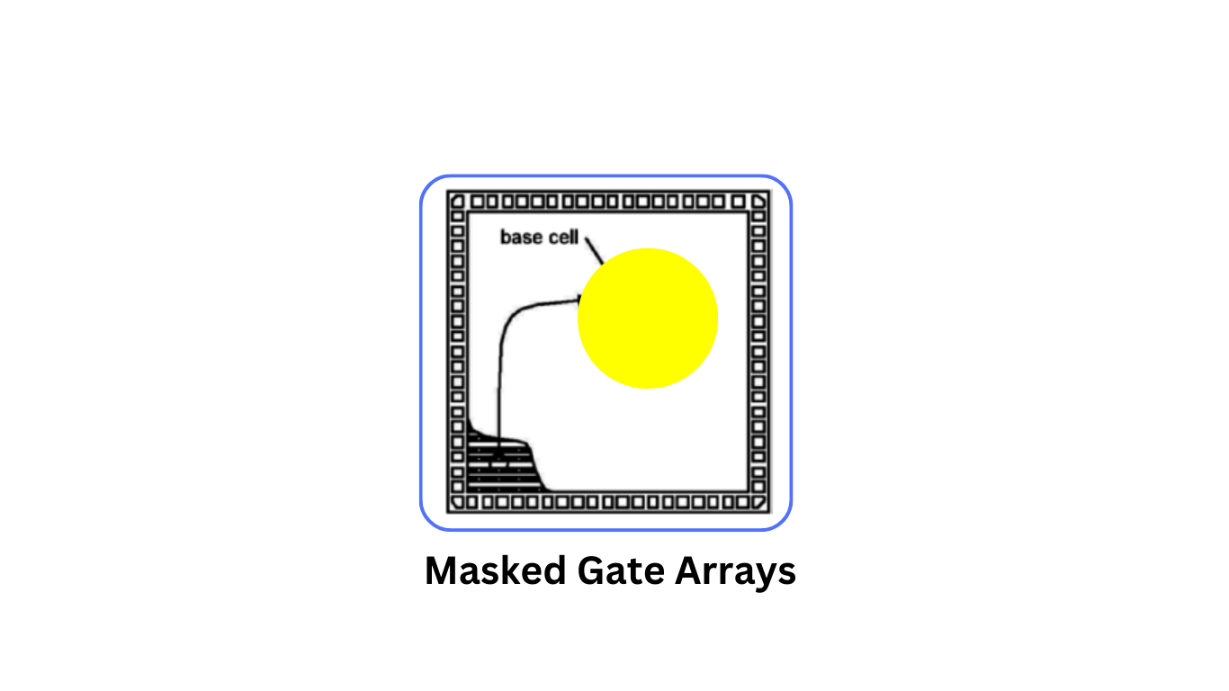
In the realm of Application-Specific Integrated Circuits (ASICs), the gate array (GA) design style represents a unique approach to ASIC customization. Gate arrays are characterized by an array of predefined base cells that are interconnected to form specific logic functions. The designer’s role in gate array customization primarily involves defining masks for creating connections and contacts between these base cells. This process of personalization is what distinguishes gate arrays, specifically masked gate arrays (MGAs), from other ASIC design styles.
Here are some key aspects of gate array design:
Masked Gate Arrays (MGAs)

The heart of the gate array design is the personalization step. In this process, the manufacturer typically keeps prefabricated wafers in stock, with the base cells already etched. The designer then specifies the connections between these base cells by defining masks for metal layers, contact points, and vias. This personalization step is what tailors the gate array to a specific application.
Types of Masked Gate Arrays
MGAs with Wiring Channels: In this type of MGA, the base cells are grouped in rows similar to standard cell designs. However, the wiring channels are fixed geometrically, and designers cannot freely choose their layout. This fixed arrangement, while reducing gate density compared to standard cells, simplifies customization.
Channelless MGAs (Sea of Gates): Channelless MGAs, also known as “Sea of Gates,” do not have dedicated wiring channels between cells. Instead, wiring is distributed across the base cells themselves. This approach allows for greater gate density compared to MGAs with wiring channels.
Structured MGAs: Structured MGAs combine matrix-like base cell arrangements with specific areas dedicated to macro cells, which might contain components like RAM or processor cores. This approach offers a blend of gate array flexibility and macro cell functionality.
Advantages of Gate Arrays
Reduced Mask Production: One of the significant advantages of gate arrays is that they require only a limited number of custom-specific masks. This results in shorter design times and higher economic efficiency when producing a small number of parts.
Shorter Time to Market: Gate arrays expedite the design process because base cells are readily available, allowing designers to focus on customization.
Disadvantages of Gate Arrays
Lower Equivalent Gate Density: Gate arrays typically exhibit a lower equivalent gate density compared to standard cell designs. This means that the price per part can be higher when gate arrays are used for very complex applications.
Challenges with Analog Circuits: Integrating analog circuits into gate arrays can be challenging and is often less practical compared to other ASIC design styles.
Gate Forest Technology Example: The “Gate Forest Technology” by IMS is provided as an example of the Sea of Gates technology. This technology offers gate arrays with a range of gate equivalents, from 2,000 to 120,000, and provides numerous I/O connections (up to 408). It also supports analog cells, making it suitable for mixed-signal applications.
In conclusion, gate array design styles offer a unique approach to ASIC customization, focusing on personalizing predefined base cells with limited mask production. While they reduce design times and can be cost-effective for smaller production runs, gate arrays may have lower gate density and pose challenges for integrating analog circuits.
How is the design implementation process different between FPGA chips and GA chips?
FPGA chips are designed through user programming, while GA chips use metal mask design and processing.
What is the two-step manufacturing process involved in gate array implementation?
The first phase results in an array of uncommitted transistors, and the second phase involves defining the metal interconnects between these transistors.
How does gate array customization take place?
Gate array customization is achieved by defining metal interconnects between the transistors of the array, which are completed after the initial chip fabrication.
What is the advantage of patterning metallic interconnects at the end of the chip fabrication process?
Patterning metallic interconnects at the end of the process allows for a short turnaround time, typically a few days to a few weeks.
What are “channels” in gate array platforms, and how are they used?
Channels are dedicated areas for inter-cell routing between rows or columns of MOS transistors. They simplify the interconnections and store interconnection patterns that perform basic logic gates.
How are multiple metal layers utilized in modern GAs for channel routing?
Multiple interconnected metal layers are used to achieve routing over the active cell areas, allowing routing channels to be removed, as seen in Sea-of-Gates (SOG) chips.
What does the term “Field Programmable Gate Array” (FPGA) refer to in the realm of programmable logic devices (PLDs)?
The term “Field Programmable Gate Array” (FPGA) refers to programmable logic devices (PLDs) with complex logic cells, where the logic function can be custom-configured using software
What is the primary advantage of using FPGAs in electronic design?
The main advantage of FPGAs is their extremely short design time because they can be configured by software without the need for additional technological steps. Designers can program and sometimes reprogram FPGAs themselves, making them attractive for small-scale projects or prototype designs of ASICs.
What are some disadvantages associated with using FPGAs compared to real ASICs (Application-Specific Integrated Circuits)?
FPGAs tend to have higher cost per part and usually lower performance compared to real ASICs.