Close Menu
  • Analog Design
    • Latest Analog Layout Interview Questions (2025)
  • Digital Design
    • Digital Electronics Interview Question(2025)
    • Top VLSI Interview Questions
  • Physical Design
    • Physical Design Interview Questions for VLSI Engineers
  • Verilog
    • Verilog Interview Questions(2024)
  • Forum
Facebook Instagram YouTube LinkedIn WhatsApp
SiliconvlsiSiliconvlsi
Ask Questions Register in Forum Login in Forum
Facebook Instagram YouTube LinkedIn WhatsApp
  • Analog Design
    • Latest Analog Layout Interview Questions (2025)
  • Digital Design
    • Digital Electronics Interview Question(2025)
    • Top VLSI Interview Questions
  • Physical Design
    • Physical Design Interview Questions for VLSI Engineers
  • Verilog
    • Verilog Interview Questions(2024)
  • Forum
SiliconvlsiSiliconvlsi
Home»Digital Design»How you will take care of power in standard cells?
Digital Design

How you will take care of power in standard cells?

siliconvlsiBy siliconvlsiMarch 24, 2022Updated:May 12, 2024No Comments1 Min Read
Facebook Pinterest LinkedIn Email WhatsApp
Share
Facebook Twitter LinkedIn Pinterest Email

How you will take care of power in standard cells?

Depending on the width(or pitch) of the metal layers the metal layer definition is defined for Standard cells.

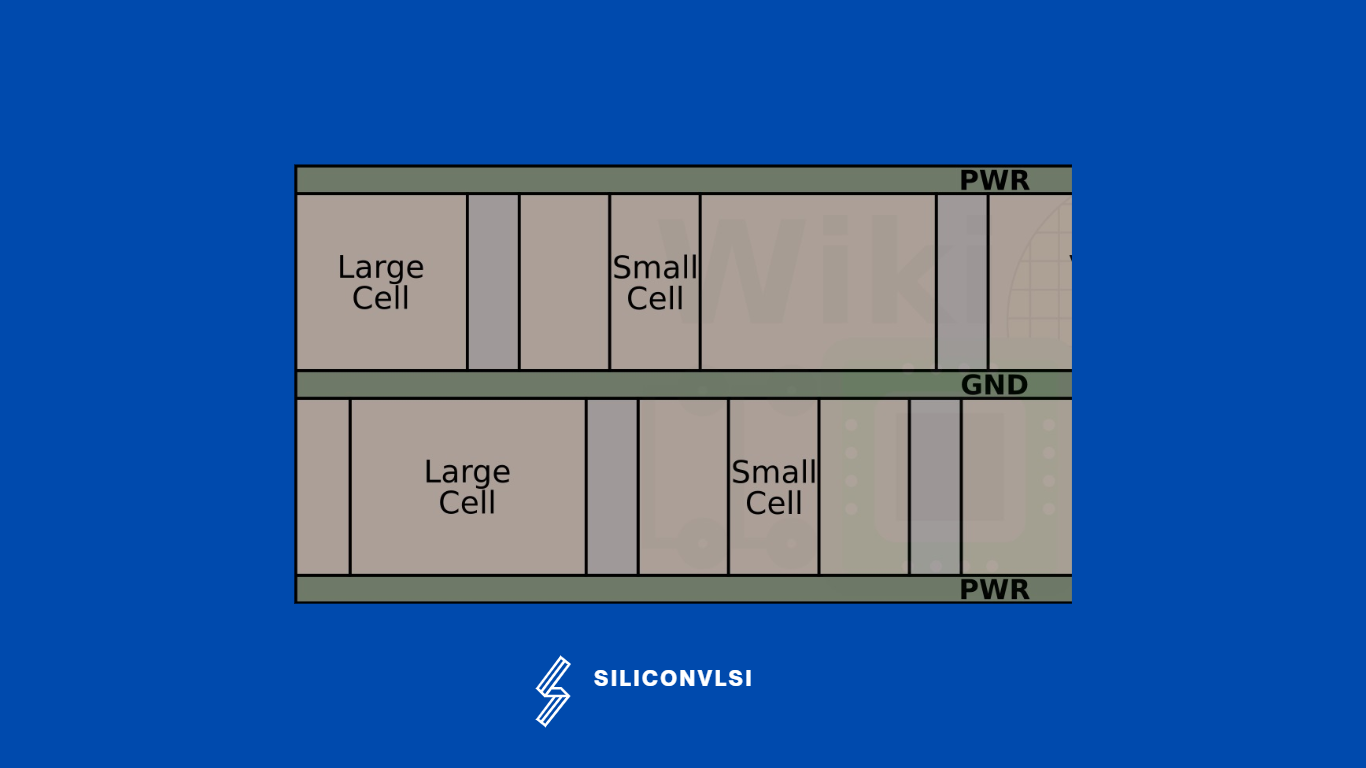
Lower metals like M0, M1, M2, and M3 are the layers used for designing the std cells, In Physical Design, we use them for power routing as well as signal routing purposes, and These layers are also called DPT layers. (only in lower nodes>16nm). The upper layers are used for routing purposes (power+signal+clock).

After certain layers, we will not route (signal routing) the design. The above layers are totally used for power. (IR drop +EM are the two things we consider for the power grid). The number of layers is depending on the design and foundry. The layer stack definition defines the layer’s information. The lower metals possess higher resistance and the higher(top) metal layers Retain a lower resistance.

The reason for deciding on metal width  is 

(R=rho*L/A)

The resistance is depending on the following factors

R=Resistance in ohms

Rho=Resistivity In ohms

L=Length in m

A=cross sectional area of m^2


Share. Facebook Twitter Pinterest LinkedIn Tumblr Email

Related Posts

Difference Between Clipper and Clamper

June 22, 2025

Understanding the Difference Between RAM Bandwidth and Clock Speed

December 1, 2024

Why is Frequency Planning so important in Module Design?

September 2, 2024
Leave A Reply Cancel Reply

Facebook X (Twitter) Instagram Pinterest Vimeo YouTube
  • About Us
  • Contact Us
  • Privacy Policy
© 2025 Siliconvlsi.

Type above and press Enter to search. Press Esc to cancel.