Analog Layout
In Analog layout there is a certain requirement for Guarding ring, well,deep-N-well, dummy devices, etc.
In a digital circuit, the gate potential is switched from rail to rail, which means the device is either completely off or completely on, and it operates in a fully depleted N-Channel. This fully depleted mode is called saturation. while In an analog circuit, the transistor is typically operated in the ohmic region, this is where the current that is allowed to flow through the device ID is proportional to VGS. to achieve this VGS operates in the range of potentials, which results in a partially depleted N-Channel.
Read also: Antenna Prevention Techniques in VLSI Design
In the ohmic mode(Linear region), the gain of the device is very sensitive to the potential difference between the gate and the substrate. A small change in the substrate potential has a large effect on the current through the device. so for that, we need to design an analog layout carefully.
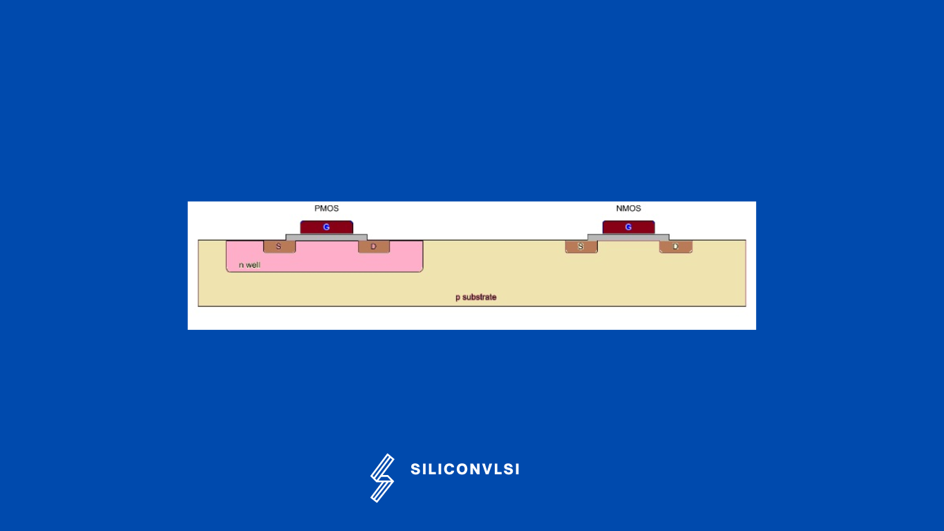
There are three main types of MOSFET devices that are used in CMOS processes.
- N-Channel devices in a P-type substrate,
- P-Channel devices in an N-well,
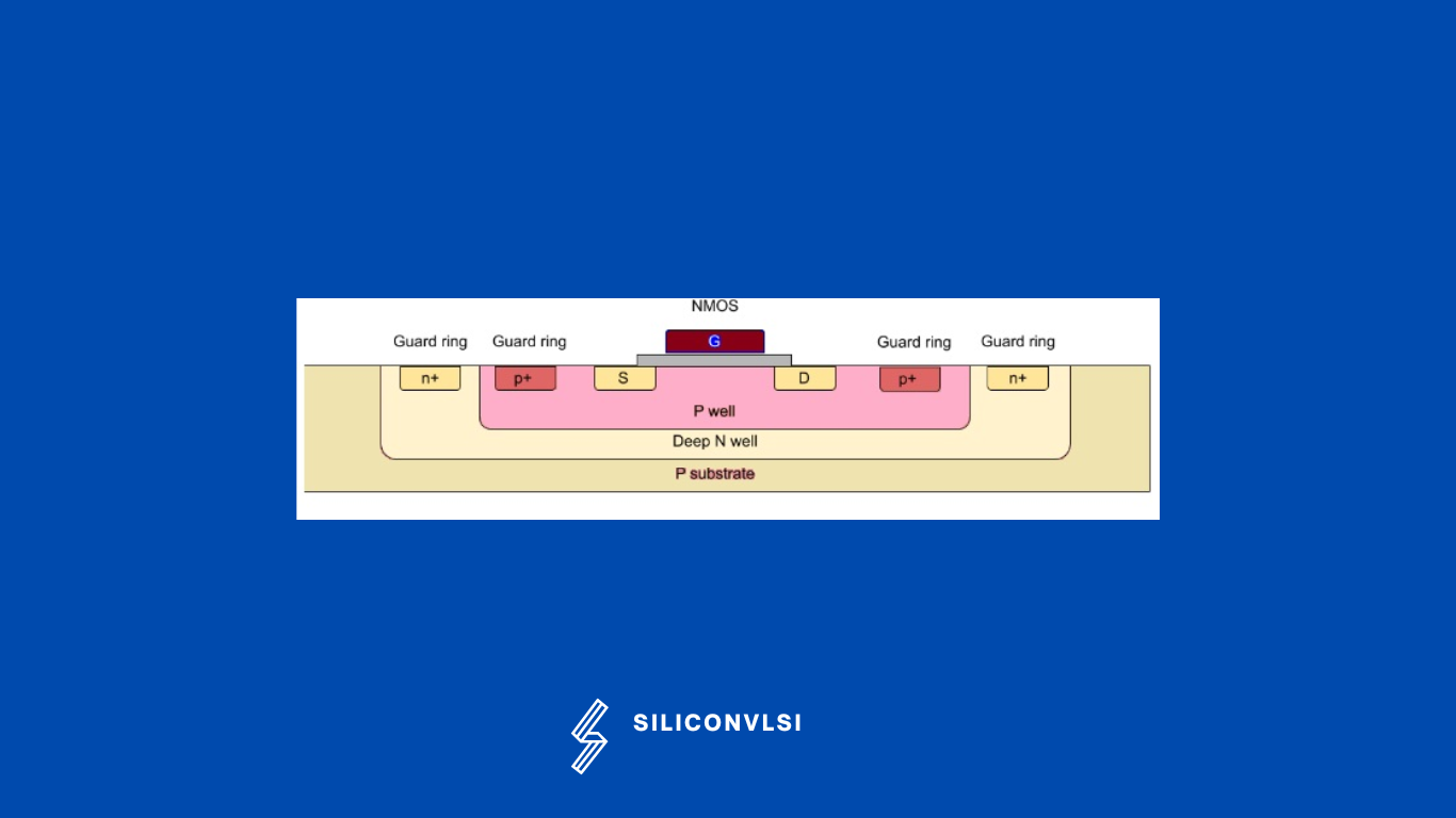
- N-Channel devices in what is called a deep N-well.
Guard rings
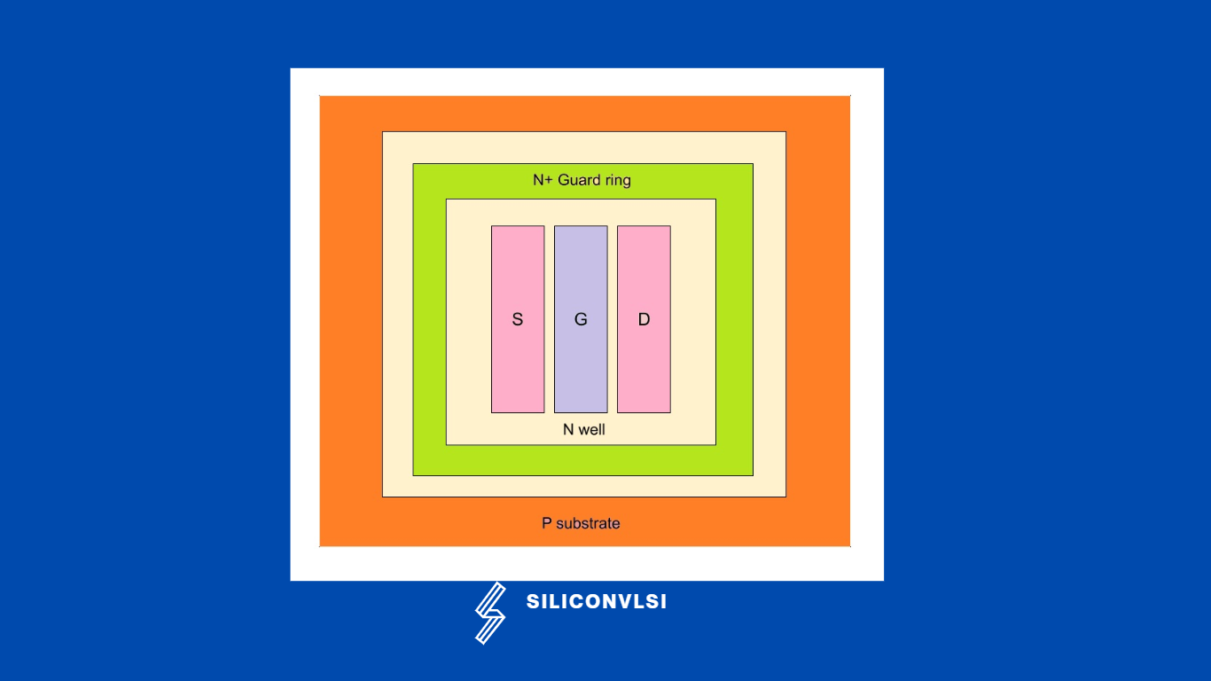
Guarding is used to collect minority charge carriers in analog devices. Most analog layouts use an extended tap structure called a “guard ring”. Guard rings are large taps that completely enclose a group of devices. It provides better device isolation as compared to taps. Guard rings more effectively isolate devices from each other, by creating a low-resistance ring.

The guard ring shape is usually repeated in metal 1 and multiple contacts are drawn connecting the metal 1 ring with the N+ ring/P+ ring. Metal 1 ensures a good connection between the guard ring and power or ground. Increasing the width of the guard ring and the number of contacts further improves the isolation. Has only disadvantage is that it will consume more area. Guard rings are particularly important in analog or mixed-signal designs, where sensitive analog circuitry is located near “noisy” digital CMOS circuitry. It provides better isolation in Layout from the outer environment. it is very effective to collect minority charge carriers from all four sides of devices.
N-wells

We use the p-substrate as a plate to design NMOS, while for PMOS we are using NWELL, In general, we use the P-substrate because it has lower doping, the higher the mobility of electrons and the higher the gain, and the higher the switching speed of transistors. So N-Channel devices can be built directly on top of this P-type substrate. P-Channel devices need an N-type substrate and to achieve this an area of N-type material is first deposited where P-Channel devices are going to be made. This N-type area is called an N-well.
Deep N-well
A deep N-well is used to isolate the device from the p substrate. Deep N-well can be used to more effectively isolate these N-channel devices. An N-well has been constructed around and beneath (hence deep) the device’s P-Well. The N-channel device operates in the P-well. Both the P-well and the deep N-well need to be tapped, but in many cases, both wells are protected with guard rings. This means that the device has two rings around it, which helps to improve the isolation of the device but requires a great deal of space in the layout.

Generally, wells, taps, and guard rings are their affect device matching. The current mirror and differential pairs require precise matching of the characteristics of different devices. A primary method of achieving good matching between two devices is to match their geometry as closely as possible. This extends to the wells, taps, and guards ring around them. A device placed close to a guard ring will have different characteristics to one placed further away(Well Proximity Effect).
Dummy devices
Why we are using dummy devices in Analog layout because…
The First reason to use dummy devices in an Analog layout is to provide the same environment around the matched devices. The Dummies device helps ensure that each device in a matching group, for instance, a current mirror has the same geometry when etched in silicon.
The second reason for using a dummy is for better optical process correction (OPC) at the last matched device pair. if we used a dummy device, we can have achieved better fabrication of the Matched device.
The third reason that dummies help matching is by reducing certain other types of layout-dependent effects (LDEs) such as well proximity effect by increasing the distance of the matched devices from the WELL edge.
![]()
For the layout design, the layout geometry of the MOSFET is created by the P-Cell(Automatic), but the position and geometry of the wells, taps, and guard rings are left to the expertise of the designer. The DRC and LVS checks will, in most cases, tell the designers where they have made mistakes, but these tools can’t measure the quality of the resulting layout. So, finally, we can say that a good layout will be generated by an expert Layout designer, not by the tool(P-cells).
What is the use of dummies in analog layout?
In many processes, designers need to insert dummy elements into the layout to ensure matching devices. Later stages of the process may require dummies at the end of each “row” for all devices. Dummies help maintain consistent geometry for each device in a matching group, such as a current mirror, during the silicon etching process.