
Double-well structure & Triple-well(Deep N-well) Structure
To understand the concept of the body terminal in transistors, it’s important to look at the cross-sectional structure of transistors, especially the well structure. The diagram in the Figure illustrates this structure. Typically, silicon wafers have a p-type substrate.
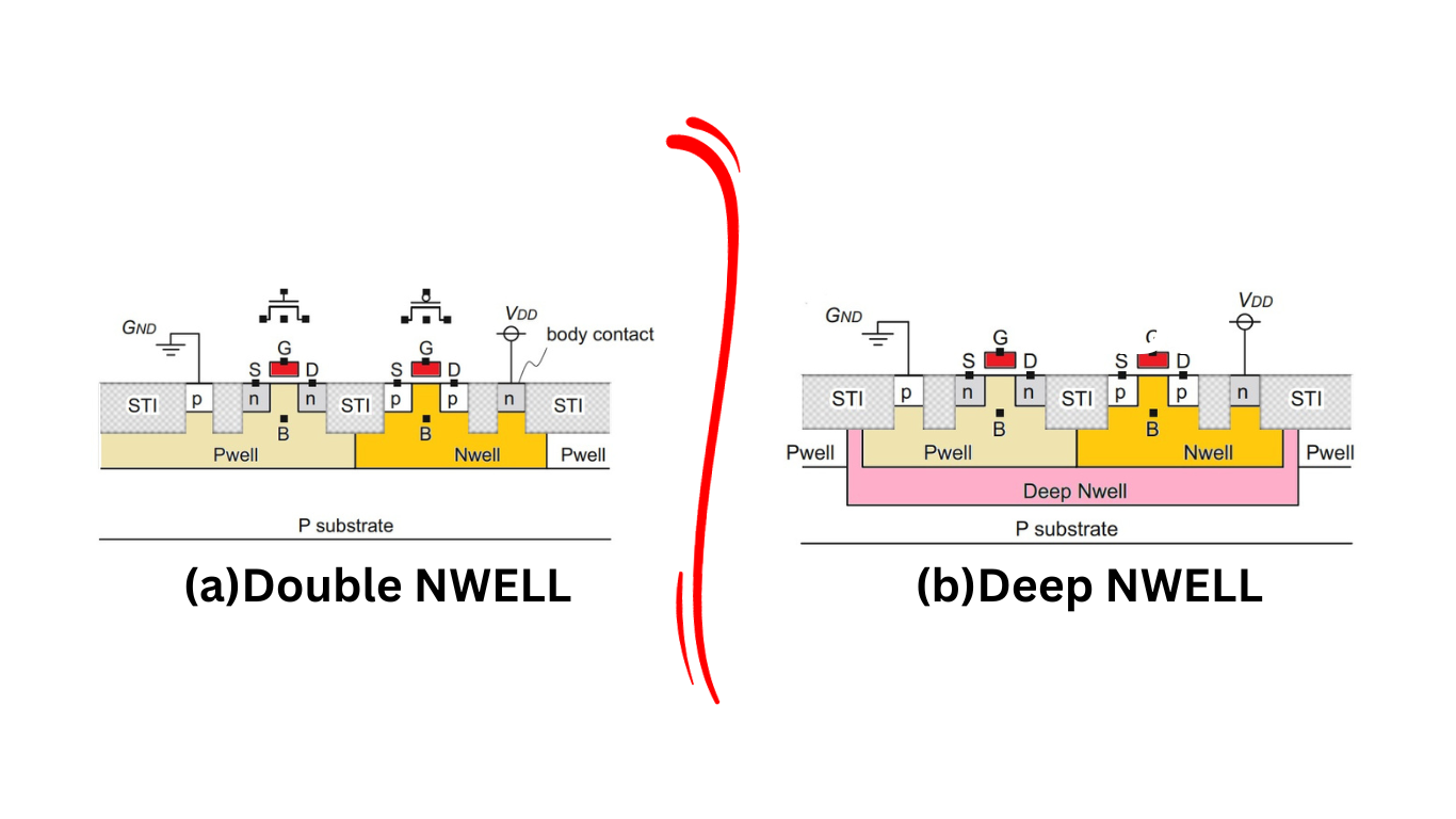
Double-Well Structure (Figure a):
- This is a fundamental structure used in MOS (Metal-Oxide-Semiconductor) fabrication.
- In an NMOS (N-channel MOS) transistor, the source and drain regions are within an n-type region that is inside a P-well.
- For a PMOS (P-channel MOS) transistor, the source and drain regions are within a p-type region inside an N-well.
- Generally, the entire P-well is connected to the ground (GND), and the N-well is connected to the supply voltage (VDD).
- Because the p-substrate (the main silicon layer) and the P-well are both conductive, the body potentials of NMOS devices are shared among all transistors.
- However, for PMOS devices, since the N-well is isolated from the P-well and p-substrate, the body potential can either be VDD or some other bias potential.
Triple-Well or Deep N-Well (DNW) Structure (Figure b):
- In this structure, a deep N-well (DNW) is introduced on top of the p-type substrate.
- The P-well and N-well, where transistors are formed, are then placed on top of this deep N-well.
- This separation of the P-well allows more control over its voltage.
- Moreover, because the circuit within the deep N-well is isolated from the p-substrate, it is less susceptible to noise that can travel through the p-substrate.
- This technique is often used to protect analog circuitry (which is sensitive to noise) from noise generated by digital circuits.
- In the diagram, “STI” stands for shallow trench isolation, which is an oxide film used to separate individual transistors.
In summary, the choice of well structure in semiconductor devices, whether it’s a double-well or triple-well structure, plays a crucial role in controlling the body potential of transistors and addressing noise-related concerns in integrated circuits.